
ECE 255 Jan 9, 2018 Lecture Instructor: Weng Cho
Description: ECE 255 Jan 9, 2018 Lecture Instructor: Weng Cho Chew Clicker Test Question 1 Have you used clicker in class before? Yes No Clicker Test Question 2 Have you registered your clicker on Black Board? Yes No ECE 255 Small Signal Model DC
Related Topics
Download Presentation
"ECE 255 Jan 9, 2018 Lecture Instructor: Weng Cho" is the property of its rightful owner. Permission is granted to download and print the materials on this website for personal, non-commercial use only, and to display it on your personal computer provided you do not modify the materials and that you retain all copyright notices contained in the materials. By downloading content from our website, you accept the terms of this agreement.
Presentation Transcript
slide1. ECE 255 Jan 9, 2018 Lecture
Instructor: Weng Cho Chew<br>
slide2. Clicker Test Question 1 Have you used clicker in class before?
Yes
No<br>
slide3. Clicker Test Question 2 Have you registered your clicker on Black Board?
Yes
No<br>
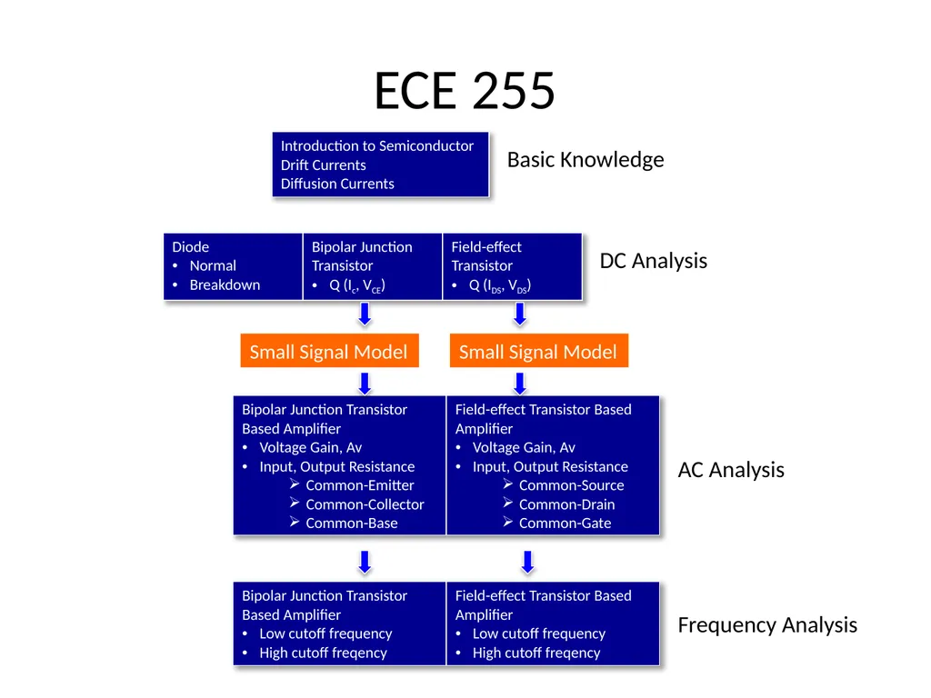
slide4. ECE 255 Small Signal Model DC Analysis Small Signal Model AC Analysis Frequency Analysis Basic Knowledge<br>
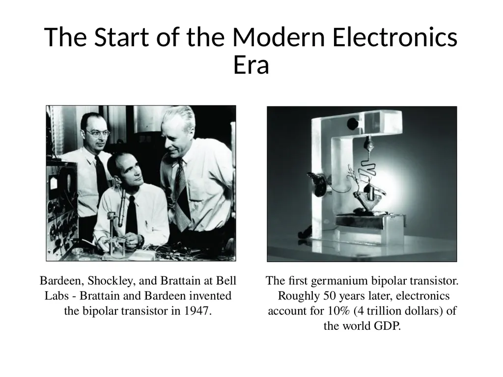
slide5. The Start of the Modern Electronics Era Bardeen, Shockley, and Brattain at Bell Labs - Brattain and Bardeen invented the bipolar transistor in 1947. The first germanium bipolar transistor. Roughly 50 years later, electronics account for 10% (4 trillion dollars) of the world GDP.<br>
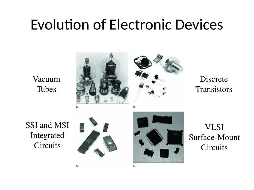
slide6. Evolution of Electronic Devices Vacuum
Tubes Discrete
Transistors SSI and MSI
Integrated
Circuits VLSI
Surface-Mount
Circuits<br>
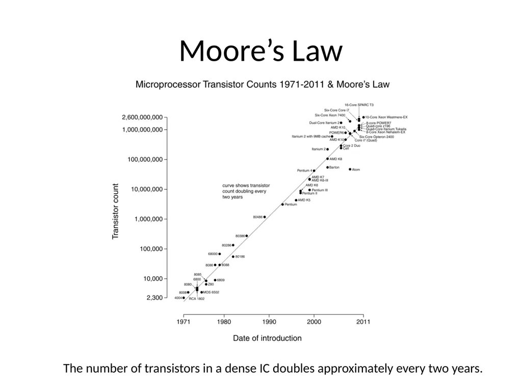
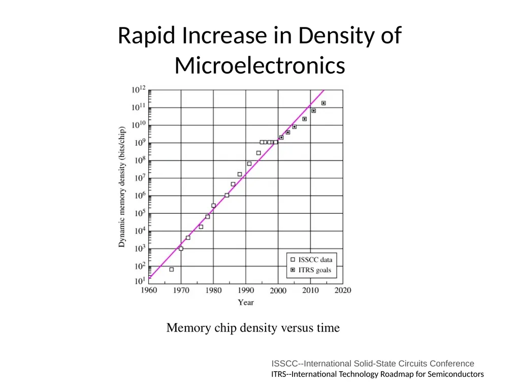
slide7. Moore’s Law The number of transistors in a dense IC doubles approximately every two years.<br>
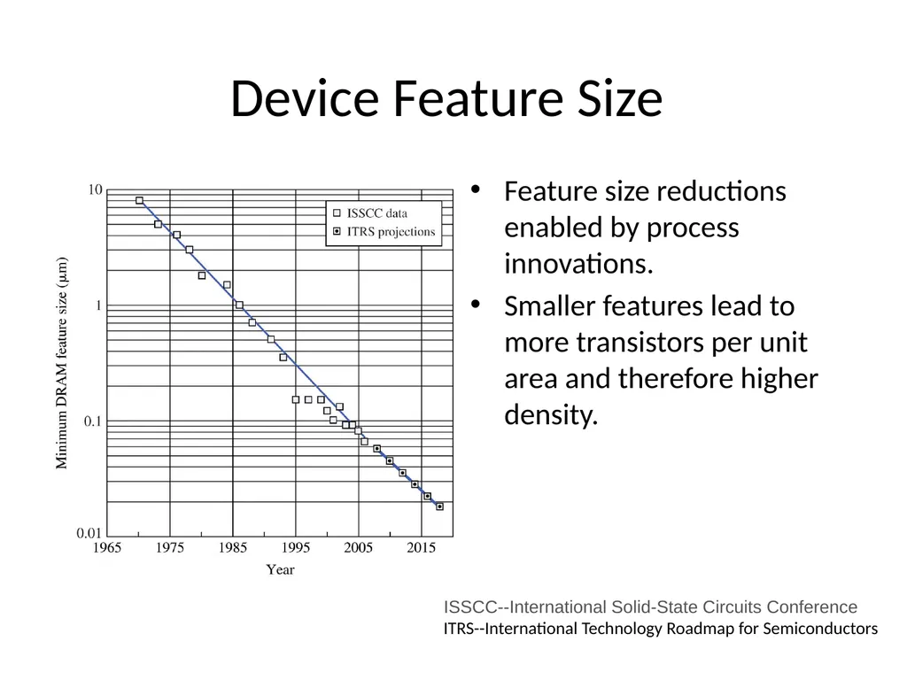
slide8. Device Feature Size Feature size reductions enabled by process innovations.
Smaller features lead to more transistors per unit area and therefore higher density. ISSCC--International Solid-State Circuits Conference
ITRS--International Technology Roadmap for Semiconductors<br>
slide9. Rapid Increase in Density of Microelectronics Memory chip density versus time ISSCC--International Solid-State Circuits Conference
ITRS--International Technology Roadmap for Semiconductors<br>
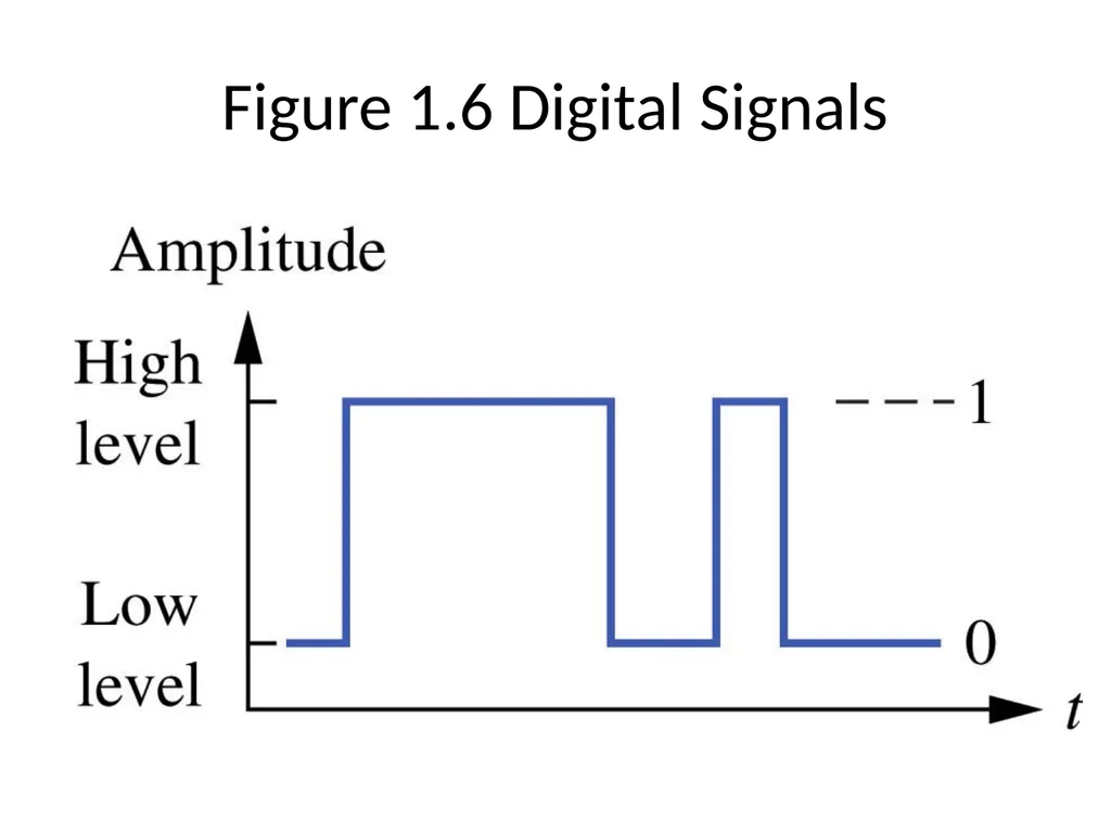
slide10. Figure 1.6 Digital Signals<br>
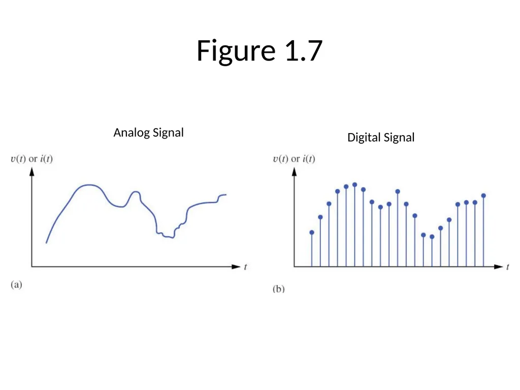
slide11. Figure 1.7 Analog Signal Digital Signal<br>
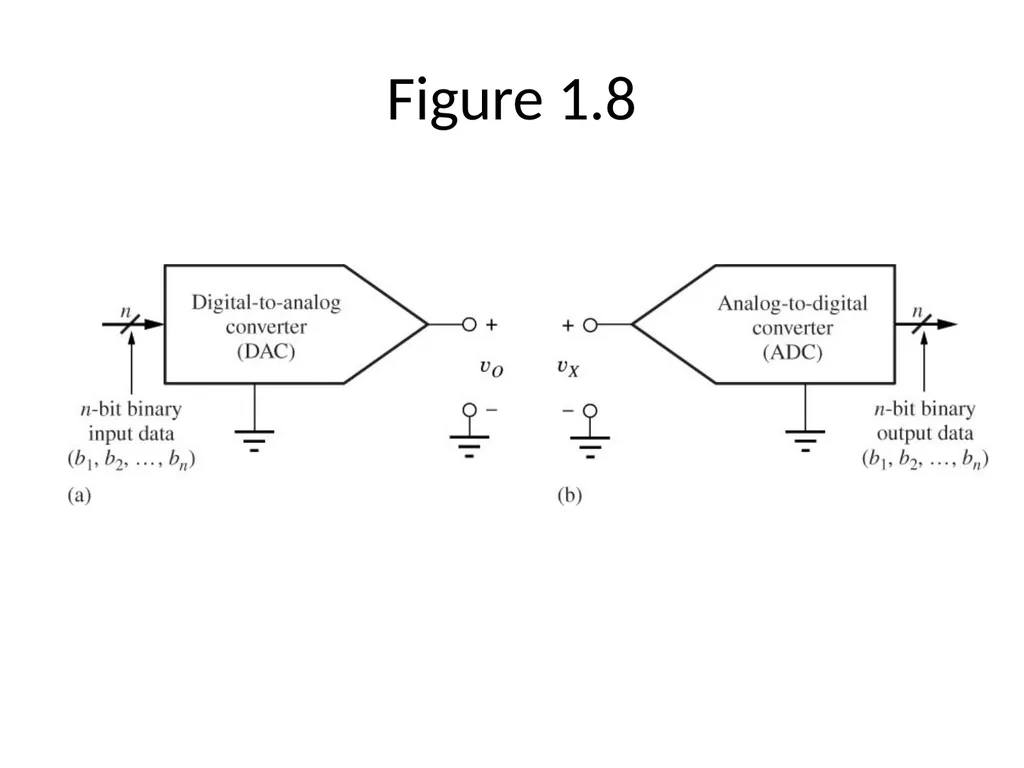
slide12. Figure 1.8<br>
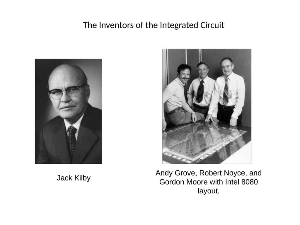
slide13. The Inventors of the Integrated Circuit Jack Kilby Andy Grove, Robert Noyce, and Gordon Moore with Intel 8080 layout.<br>
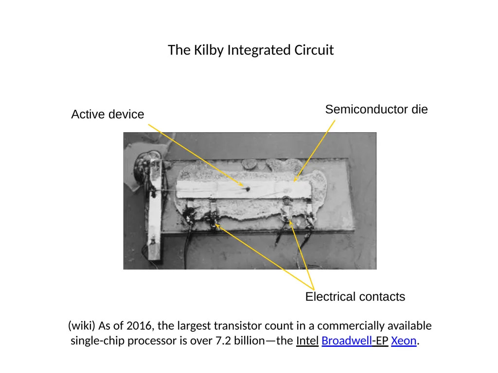
slide14. The Kilby Integrated Circuit Semiconductor die Active device Electrical contacts (wiki) As of 2016, the largest transistor count in a commercially available
single-chip processor is over 7.2 billion—the Intel Broadwell-EP Xeon.<br>
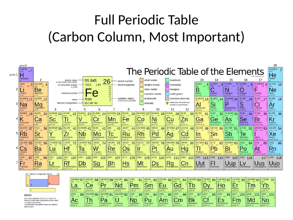
slide15. Full Periodic Table (Carbon Column, Most Important)<br>
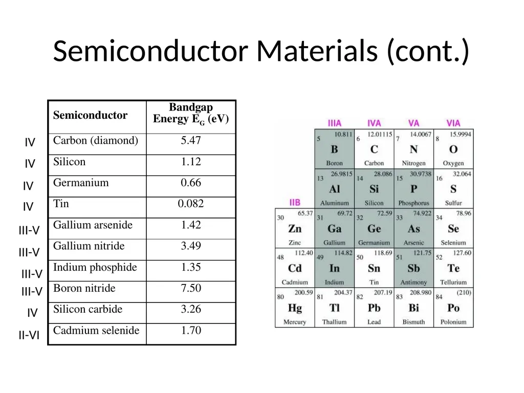
slide16. Semiconductor Materials (cont.) IV IV IV IV III-V III-V III-V III-V IV II-VI<br>
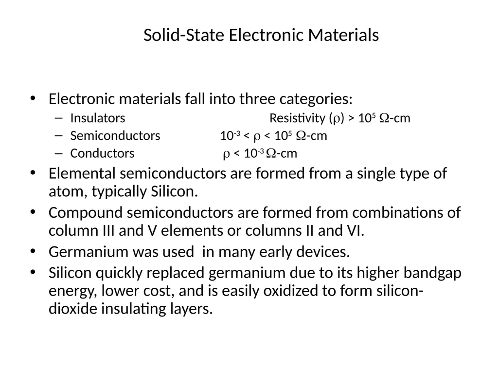
slide17. Solid-State Electronic Materials Electronic materials fall into three categories:
Insulators Resistivity () > 105 -cm
Semiconductors 10-3 < < 105 -cm
Conductors < 10-3 -cm
Elemental semiconductors are formed from a single type of atom, typically Silicon.
Compound semiconductors are formed from combinations of column III and V elements or columns II and VI.
Germanium was used in many early devices.
Silicon quickly replaced germanium due to its higher bandgap energy, lower cost, and is easily oxidized to form silicon-dioxide insulating layers.<br>
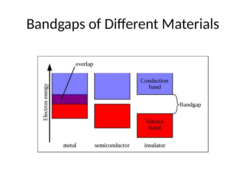
slide18. Bandgaps of Different Materials<br>
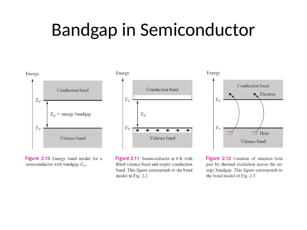
slide19. Bandgap in Semiconductor<br>
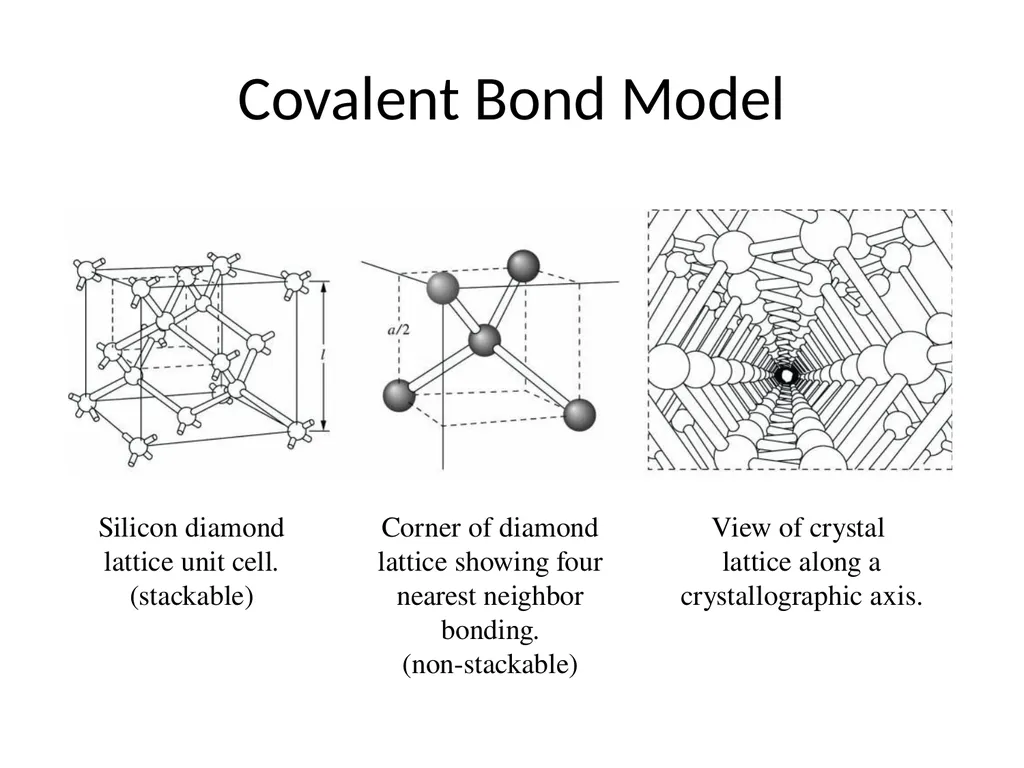
slide20. Covalent Bond Model Silicon diamond lattice unit cell.
(stackable) Corner of diamond lattice showing four nearest neighbor bonding.
(non-stackable) View of crystal lattice along a crystallographic axis.<br>
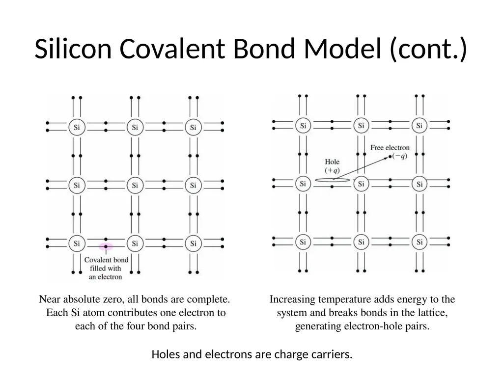
slide21. Silicon Covalent Bond Model (cont.) Near absolute zero, all bonds are complete. Each Si atom contributes one electron to each of the four bond pairs. Increasing temperature adds energy to the system and breaks bonds in the lattice, generating electron-hole pairs. Holes and electrons are charge carriers.<br>
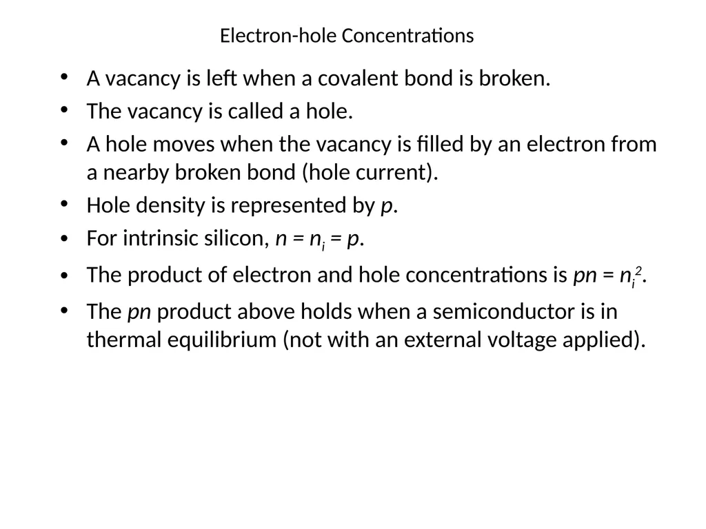
slide22. Electron-hole Concentrations A vacancy is left when a covalent bond is broken.
The vacancy is called a hole.
A hole moves when the vacancy is filled by an electron from a nearby broken bond (hole current).
Hole density is represented by p.
For intrinsic silicon, n = ni = p.
The product of electron and hole concentrations is pn = ni2.
The pn product above holds when a semiconductor is in thermal equilibrium (not with an external voltage applied).<br>
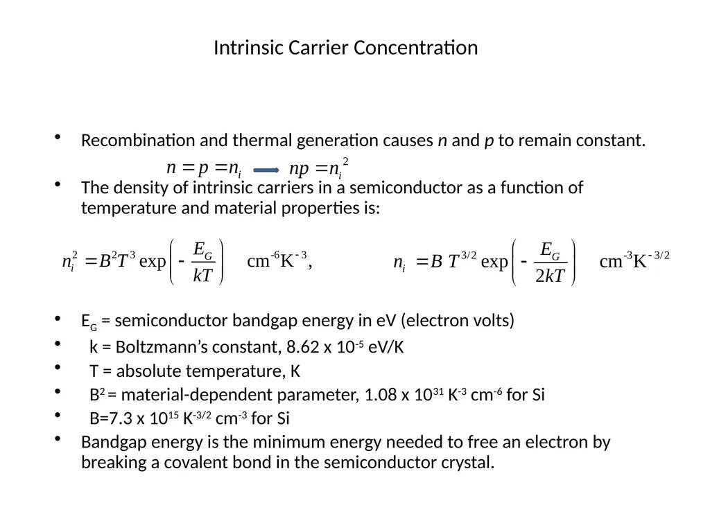
slide23. Intrinsic Carrier Concentration Recombination and thermal generation causes n and p to remain constant.
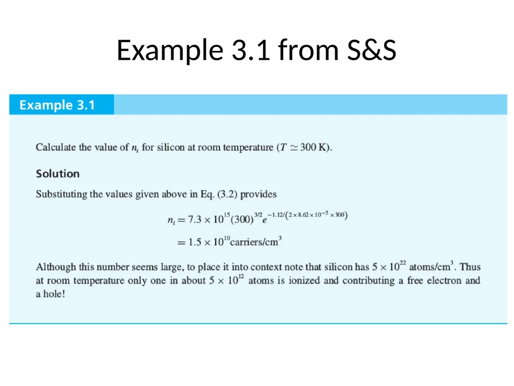
The density of intrinsic carriers in a semiconductor as a function of temperature and material properties is:
EG = semiconductor bandgap energy in eV (electron volts)
k = Boltzmann’s constant, 8.62 x 10⁻⁵ eV/K
T = absolute temperature, K
B2 = material-dependent parameter, 1.08 x 1031 K-3 cm-6 for Si
B=7.3 x 10¹⁵ K-3/2 cm-3 for Si
Bandgap energy is the minimum energy needed to free an electron by breaking a covalent bond in the semiconductor crystal.<br>
slide24. Example 3.1 from S&S<br>
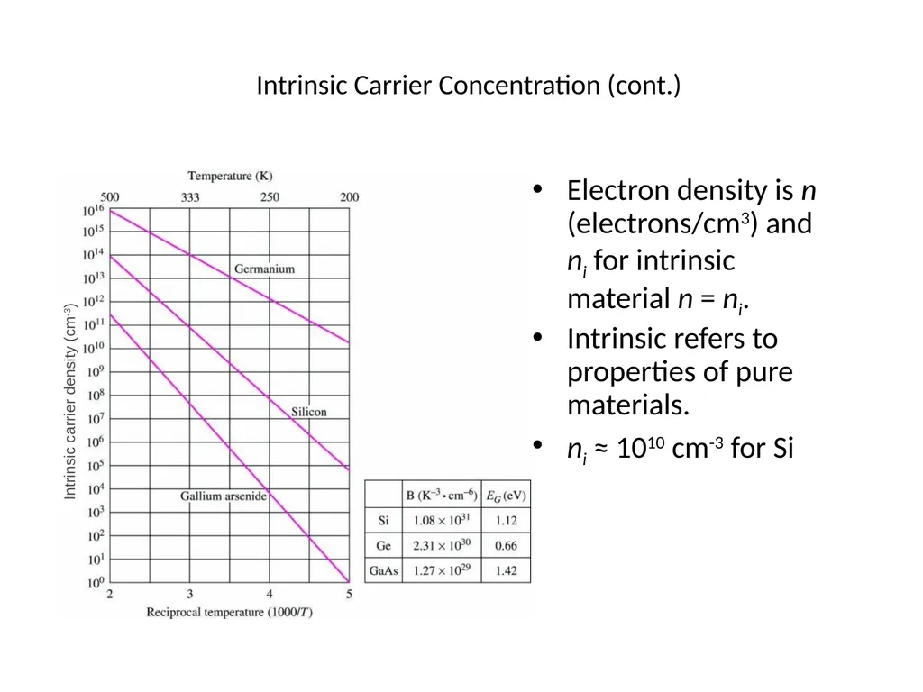
slide25. Intrinsic Carrier Concentration (cont.) Electron density is n (electrons/cm3) and ni for intrinsic material n = ni.
Intrinsic refers to properties of pure materials.
ni ≈ 1010 cm-3 for Si Intrinsic carrier density (cm-3)<br>
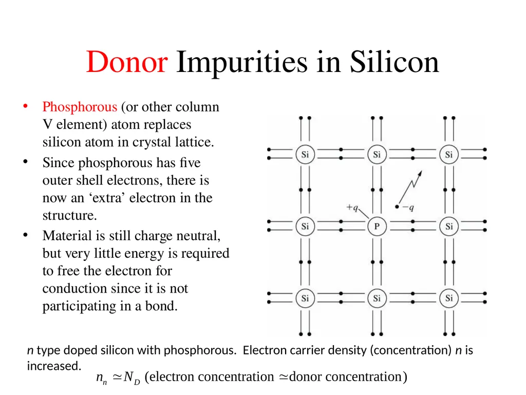
slide26. Donor Impurities in Silicon Phosphorous (or other column V element) atom replaces silicon atom in crystal lattice.
Since phosphorous has five outer shell electrons, there is now an ‘extra’ electron in the structure.
Material is still charge neutral, but very little energy is required to free the electron for conduction since it is not participating in a bond. n type doped silicon with phosphorous. Electron carrier density (concentration) n is increased.<br>
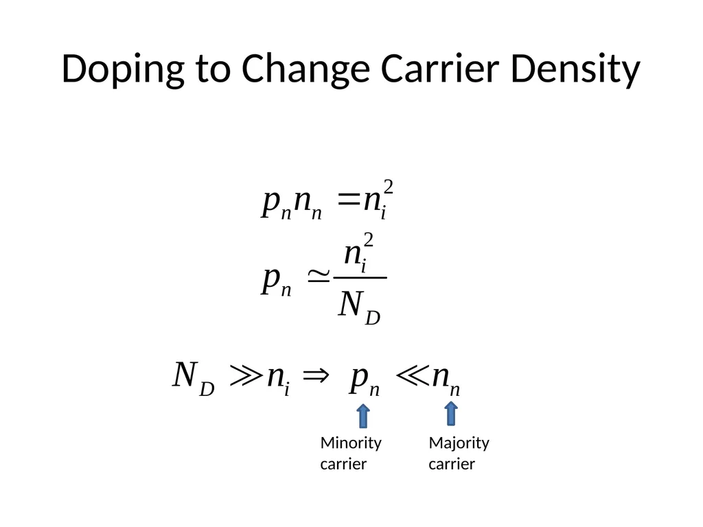
slide27. Doping to Change Carrier Density Minority carrier Majority carrier<br>
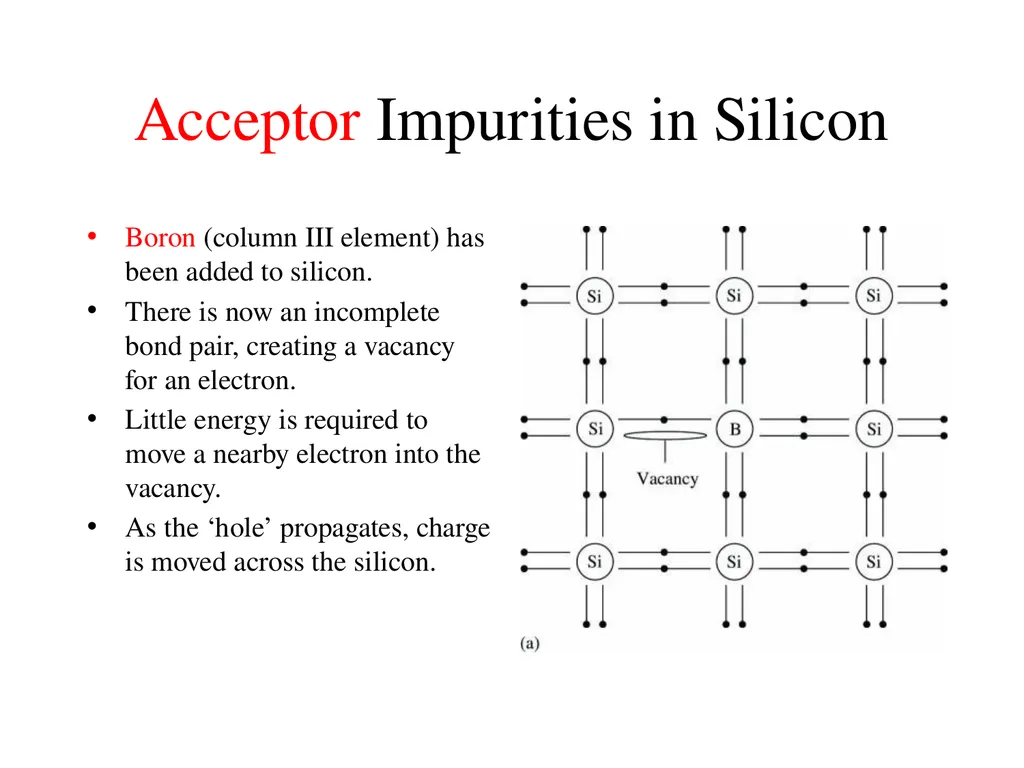
slide28. Acceptor Impurities in Silicon Boron (column III element) has been added to silicon.
There is now an incomplete bond pair, creating a vacancy for an electron.
Little energy is required to move a nearby electron into the vacancy.
As the ‘hole’ propagates, charge is moved across the silicon.<br>
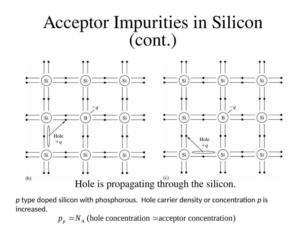
slide29. Acceptor Impurities in Silicon (cont.) Hole is propagating through the silicon. p type doped silicon with phosphorous. Hole carrier density or concentration p is increased.<br>
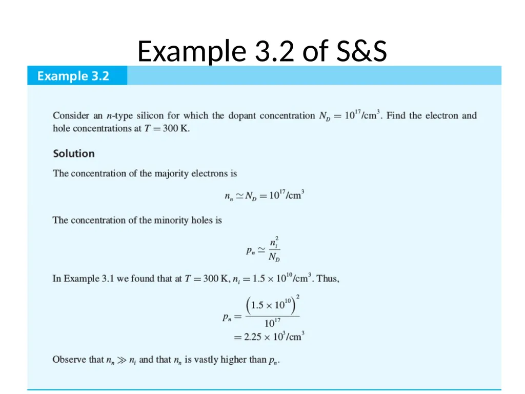
slide30. Example 3.2 of S&S<br>
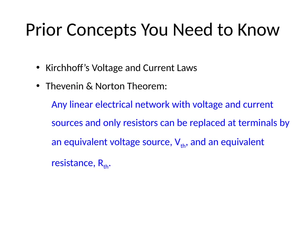
slide31. Prior Concepts You Need to Know Kirchhoff’s Voltage and Current Laws
Thevenin & Norton Theorem:
Any linear electrical network with voltage and current sources and only resistors can be replaced at terminals by an equivalent voltage source, Vth, and an equivalent resistance, Rth.<br>
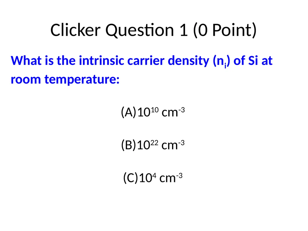
slide32. Clicker Question 1 (0 Point) What is the intrinsic carrier density (ni) of Si at room temperature:
1010 cm-3
1022 cm-3
104 cm-3<br>
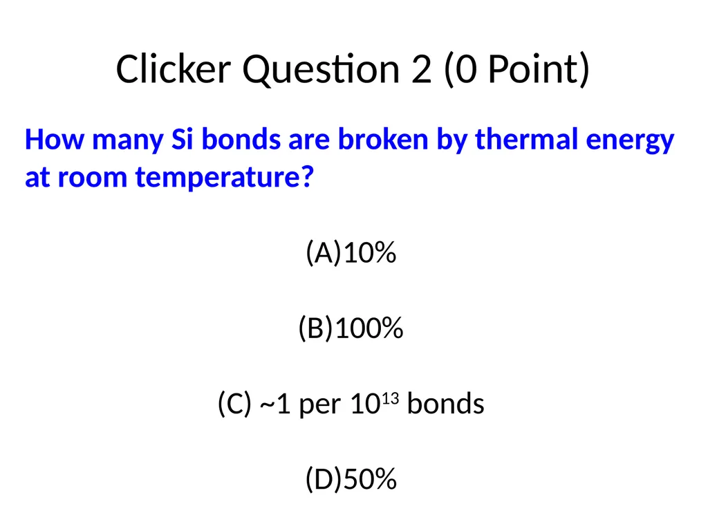
slide33. Clicker Question 2 (0 Point) How many Si bonds are broken by thermal energy at room temperature?
10%
100%
~1 per 1013 bonds
50%<br>
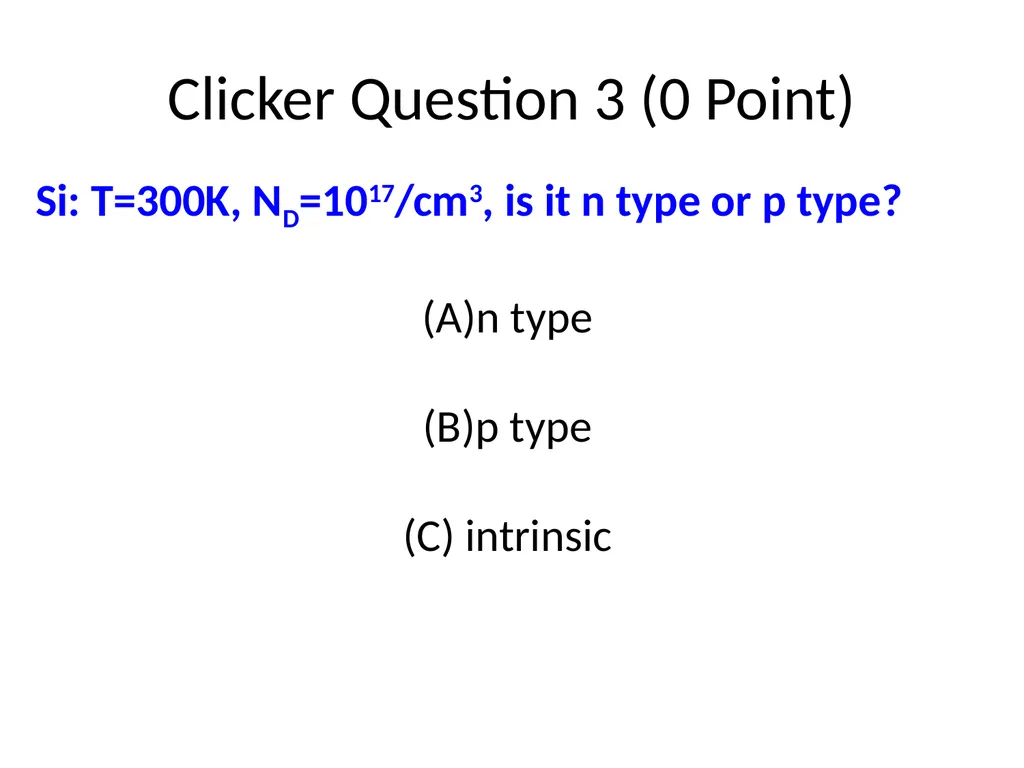
slide34. Clicker Question 3 (0 Point) Si: T=300K, ND=1017/cm3, is it n type or p type?
n type
p type
intrinsic<br>
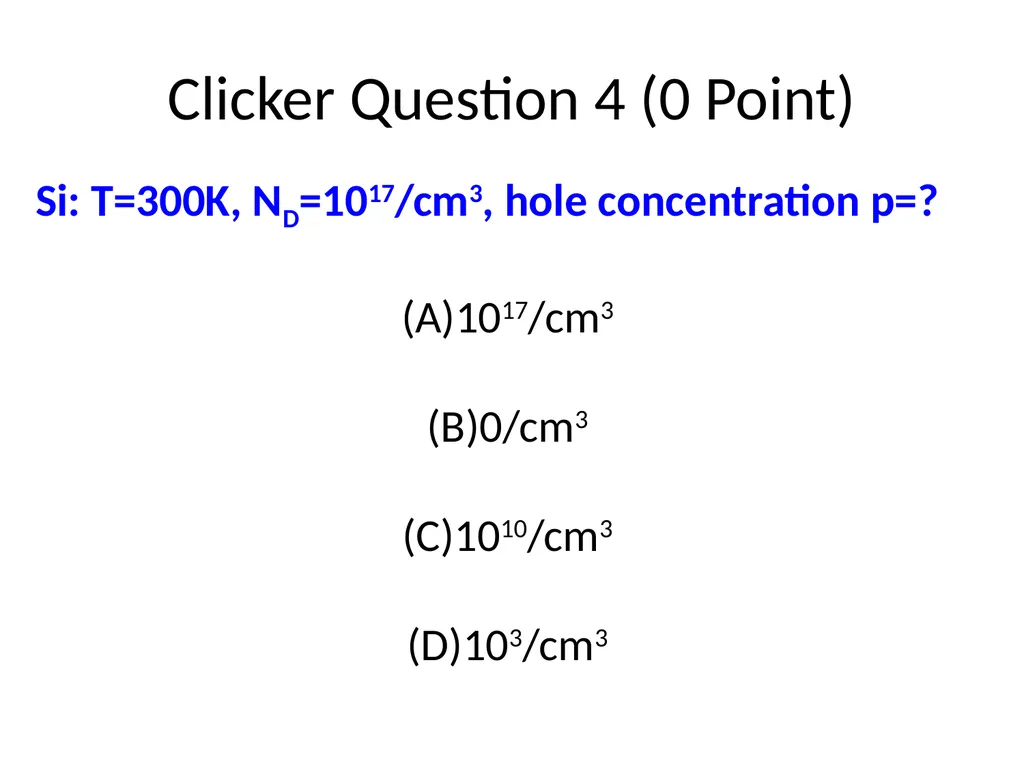
slide35. Clicker Question 4 (0 Point) Si: T=300K, ND=1017/cm3, hole concentration p=?
1017/cm3
0/cm3
1010/cm3
103/cm3<br>
Instructor: Weng Cho Chew<br>
slide2. Clicker Test Question 1 Have you used clicker in class before?
Yes
No<br>
slide3. Clicker Test Question 2 Have you registered your clicker on Black Board?
Yes
No<br>
slide4. ECE 255 Small Signal Model DC Analysis Small Signal Model AC Analysis Frequency Analysis Basic Knowledge<br>
slide5. The Start of the Modern Electronics Era Bardeen, Shockley, and Brattain at Bell Labs - Brattain and Bardeen invented the bipolar transistor in 1947. The first germanium bipolar transistor. Roughly 50 years later, electronics account for 10% (4 trillion dollars) of the world GDP.<br>
slide6. Evolution of Electronic Devices Vacuum
Tubes Discrete
Transistors SSI and MSI
Integrated
Circuits VLSI
Surface-Mount
Circuits<br>
slide7. Moore’s Law The number of transistors in a dense IC doubles approximately every two years.<br>
slide8. Device Feature Size Feature size reductions enabled by process innovations.
Smaller features lead to more transistors per unit area and therefore higher density. ISSCC--International Solid-State Circuits Conference
ITRS--International Technology Roadmap for Semiconductors<br>
slide9. Rapid Increase in Density of Microelectronics Memory chip density versus time ISSCC--International Solid-State Circuits Conference
ITRS--International Technology Roadmap for Semiconductors<br>
slide10. Figure 1.6 Digital Signals<br>
slide11. Figure 1.7 Analog Signal Digital Signal<br>
slide12. Figure 1.8<br>
slide13. The Inventors of the Integrated Circuit Jack Kilby Andy Grove, Robert Noyce, and Gordon Moore with Intel 8080 layout.<br>
slide14. The Kilby Integrated Circuit Semiconductor die Active device Electrical contacts (wiki) As of 2016, the largest transistor count in a commercially available
single-chip processor is over 7.2 billion—the Intel Broadwell-EP Xeon.<br>
slide15. Full Periodic Table (Carbon Column, Most Important)<br>
slide16. Semiconductor Materials (cont.) IV IV IV IV III-V III-V III-V III-V IV II-VI<br>
slide17. Solid-State Electronic Materials Electronic materials fall into three categories:
Insulators Resistivity () > 105 -cm
Semiconductors 10-3 < < 105 -cm
Conductors < 10-3 -cm
Elemental semiconductors are formed from a single type of atom, typically Silicon.
Compound semiconductors are formed from combinations of column III and V elements or columns II and VI.
Germanium was used in many early devices.
Silicon quickly replaced germanium due to its higher bandgap energy, lower cost, and is easily oxidized to form silicon-dioxide insulating layers.<br>
slide18. Bandgaps of Different Materials<br>
slide19. Bandgap in Semiconductor<br>
slide20. Covalent Bond Model Silicon diamond lattice unit cell.
(stackable) Corner of diamond lattice showing four nearest neighbor bonding.
(non-stackable) View of crystal lattice along a crystallographic axis.<br>
slide21. Silicon Covalent Bond Model (cont.) Near absolute zero, all bonds are complete. Each Si atom contributes one electron to each of the four bond pairs. Increasing temperature adds energy to the system and breaks bonds in the lattice, generating electron-hole pairs. Holes and electrons are charge carriers.<br>
slide22. Electron-hole Concentrations A vacancy is left when a covalent bond is broken.
The vacancy is called a hole.
A hole moves when the vacancy is filled by an electron from a nearby broken bond (hole current).
Hole density is represented by p.
For intrinsic silicon, n = ni = p.
The product of electron and hole concentrations is pn = ni2.
The pn product above holds when a semiconductor is in thermal equilibrium (not with an external voltage applied).<br>
slide23. Intrinsic Carrier Concentration Recombination and thermal generation causes n and p to remain constant.
The density of intrinsic carriers in a semiconductor as a function of temperature and material properties is:
EG = semiconductor bandgap energy in eV (electron volts)
k = Boltzmann’s constant, 8.62 x 10⁻⁵ eV/K
T = absolute temperature, K
B2 = material-dependent parameter, 1.08 x 1031 K-3 cm-6 for Si
B=7.3 x 10¹⁵ K-3/2 cm-3 for Si
Bandgap energy is the minimum energy needed to free an electron by breaking a covalent bond in the semiconductor crystal.<br>
slide24. Example 3.1 from S&S<br>
slide25. Intrinsic Carrier Concentration (cont.) Electron density is n (electrons/cm3) and ni for intrinsic material n = ni.
Intrinsic refers to properties of pure materials.
ni ≈ 1010 cm-3 for Si Intrinsic carrier density (cm-3)<br>
slide26. Donor Impurities in Silicon Phosphorous (or other column V element) atom replaces silicon atom in crystal lattice.
Since phosphorous has five outer shell electrons, there is now an ‘extra’ electron in the structure.
Material is still charge neutral, but very little energy is required to free the electron for conduction since it is not participating in a bond. n type doped silicon with phosphorous. Electron carrier density (concentration) n is increased.<br>
slide27. Doping to Change Carrier Density Minority carrier Majority carrier<br>
slide28. Acceptor Impurities in Silicon Boron (column III element) has been added to silicon.
There is now an incomplete bond pair, creating a vacancy for an electron.
Little energy is required to move a nearby electron into the vacancy.
As the ‘hole’ propagates, charge is moved across the silicon.<br>
slide29. Acceptor Impurities in Silicon (cont.) Hole is propagating through the silicon. p type doped silicon with phosphorous. Hole carrier density or concentration p is increased.<br>
slide30. Example 3.2 of S&S<br>
slide31. Prior Concepts You Need to Know Kirchhoff’s Voltage and Current Laws
Thevenin & Norton Theorem:
Any linear electrical network with voltage and current sources and only resistors can be replaced at terminals by an equivalent voltage source, Vth, and an equivalent resistance, Rth.<br>
slide32. Clicker Question 1 (0 Point) What is the intrinsic carrier density (ni) of Si at room temperature:
1010 cm-3
1022 cm-3
104 cm-3<br>
slide33. Clicker Question 2 (0 Point) How many Si bonds are broken by thermal energy at room temperature?
10%
100%
~1 per 1013 bonds
50%<br>
slide34. Clicker Question 3 (0 Point) Si: T=300K, ND=1017/cm3, is it n type or p type?
n type
p type
intrinsic<br>
slide35. Clicker Question 4 (0 Point) Si: T=300K, ND=1017/cm3, hole concentration p=?
1017/cm3
0/cm3
1010/cm3
103/cm3<br>