
Introduction to Nanoparticles and Nanostructures












Description: Introduction to Nanoparticles and Nanostructures Outline Definition and Examples Physical Properties Size Crystal Structure Melting Point Mechanical Strength Optical Properties Surface Plasmons Quantum Confinement Effects Electrical
Related Topics
Download Presentation
"Introduction to Nanoparticles and Nanostructures" is the property of its rightful owner. Permission is granted to download and print the materials on this website for personal, non-commercial use only, and to display it on your personal computer provided you do not modify the materials and that you retain all copyright notices contained in the materials. By downloading content from our website, you accept the terms of this agreement.
Presentation Transcript
slide1. Introduction to Nanoparticles and Nanostructures<br>
slide2. Outline Definition and Examples
Physical Properties
Size
Crystal Structure
Melting Point
Mechanical Strength
Optical Properties
Surface Plasmons
Quantum Confinement Effects
Electrical Properties
Health Concerns<br>
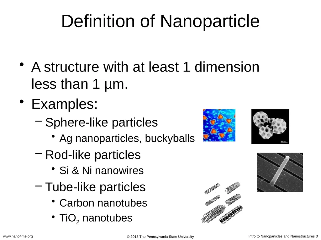
slide3. Definition of Nanoparticle A structure with at least 1 dimension less than 1 µm.
Examples:
Sphere-like particles
Ag nanoparticles, buckyballs
Rod-like particles
Si & Ni nanowires
Tube-like particles
Carbon nanotubes
TiO2 nanotubes<br>
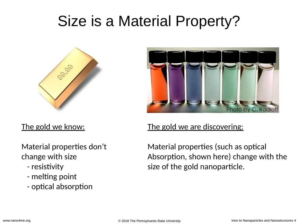
slide4. Size is a Material Property? The gold we know:
Material properties don’t change with size
- resistivity
- melting point
- optical absorption The gold we are discovering:
Material properties (such as optical
Absorption, shown here) change with the size of the gold nanoparticle.<br>
slide5. Outline Definition and Examples
Physical Properties
Size
Crystal Structure
Melting Point
Mechanical Strength
Optical Properties
Electrical Properties
Health Concerns<br>
slide6. Unique Characteristics of Nanoparticles Large surface to volume ratio
High percentage of atoms/molecules on the surface
Surface forces are very important, while bulk forces are not as important.
Metal nanoparticles have unique light scattering properties and exhibit plasmon resonance.
Semiconductor nanoparticles may exhibit confined energy states in their electronic band structure (e.g., quantum dots)
Can have unique chemical and physical properties
Same size scale as many biological structures<br>
slide7. Examples of Unusual Properties Lowered phase transition temps
Increased mechanical strength
Different optical properties
Altered electrical conductivity
Magnetic properties
Self-purification and self-perfection<br>
slide8. Physical Properties of Nanoparticles Physical properties of nanoparticles are dependent on:
Size
Shape (spheres, rods, platelets, etc.)
Composition
Crystal Structure (FCC, BCC, etc.)
Surface ligands or capping agents
The medium in which they are dispersed<br>
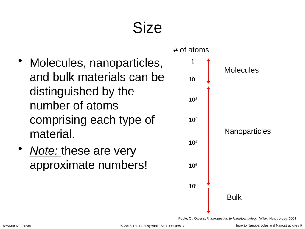
slide9. Size Molecules, nanoparticles, and bulk materials can be distinguished by the number of atoms comprising each type of material.
Note: these are very approximate numbers! Poole, C., Owens, F. Introduction to Nanotechnology. Wiley, New Jersey. 2003 1 10 102 103 104 105 106 Molecules Nanoparticles Bulk # of atoms<br>
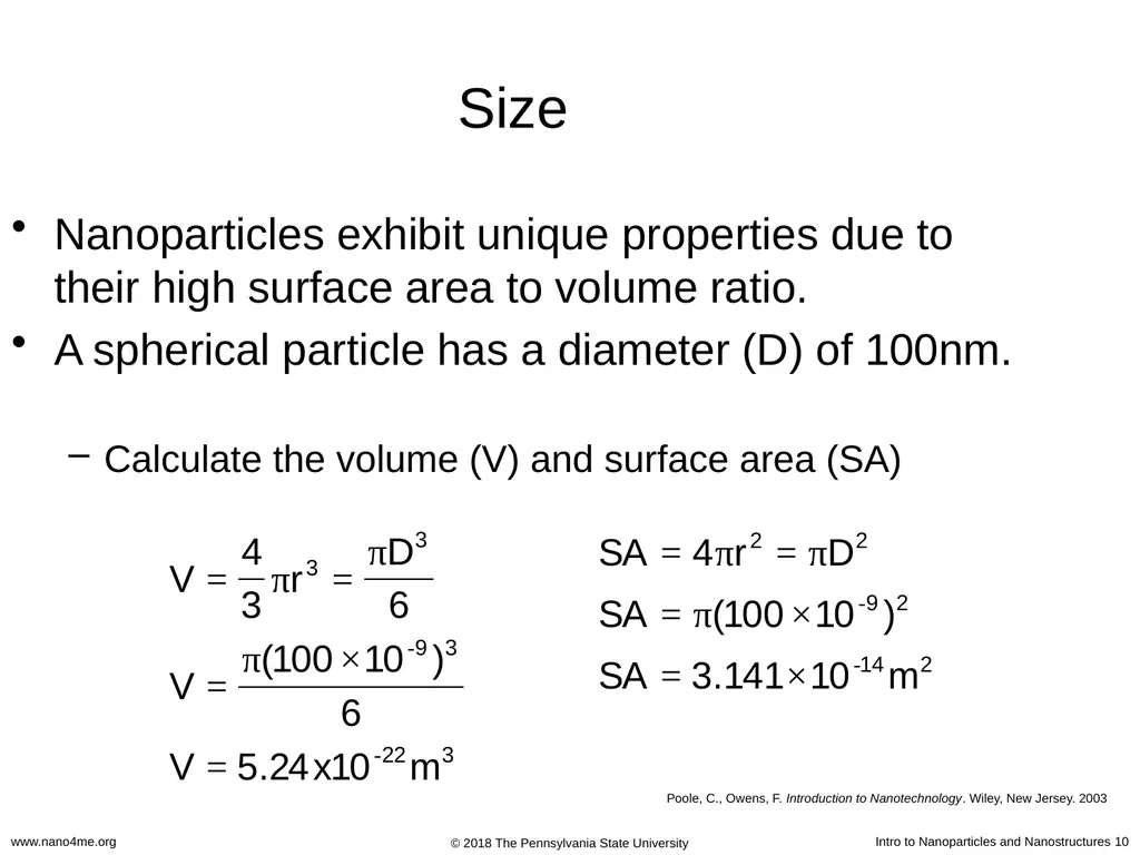
slide10. Size Nanoparticles exhibit unique properties due to their high surface area to volume ratio.
A spherical particle has a diameter (D) of 100nm.
Calculate the volume (V) and surface area (SA) Poole, C., Owens, F. Introduction to Nanotechnology. Wiley, New Jersey. 2003<br>
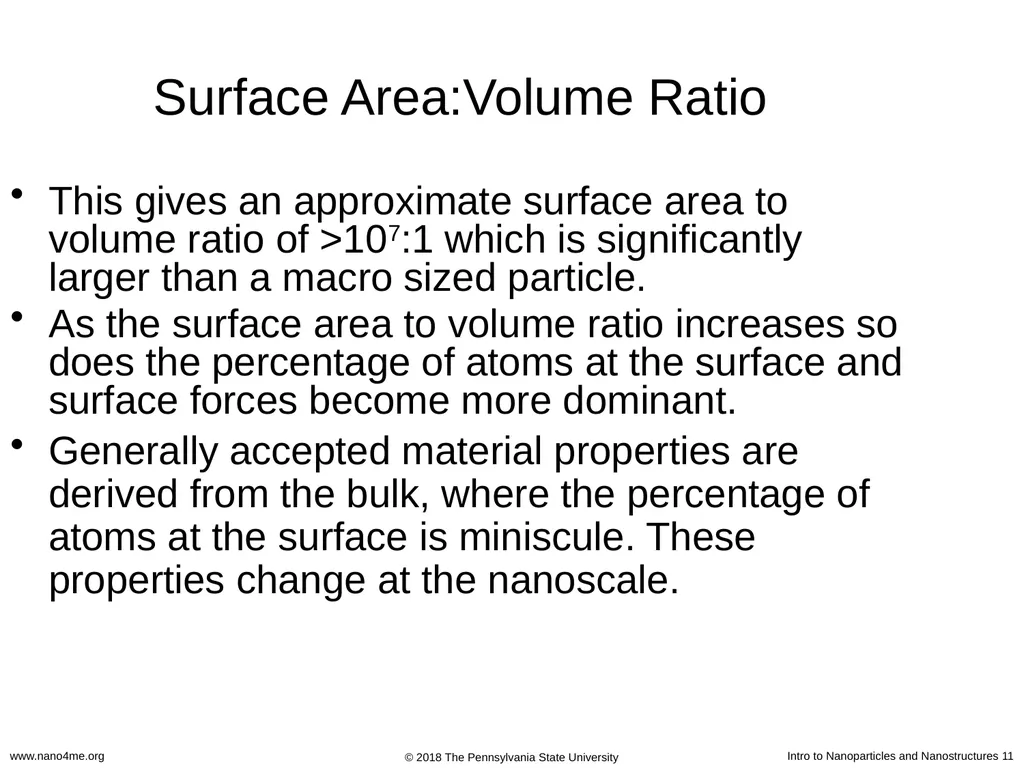
slide11. Surface Area:Volume Ratio This gives an approximate surface area to volume ratio of >107:1 which is significantly larger than a macro sized particle.
As the surface area to volume ratio increases so does the percentage of atoms at the surface and surface forces become more dominant.
Generally accepted material properties are derived from the bulk, where the percentage of atoms at the surface is miniscule. These properties change at the nanoscale.<br>
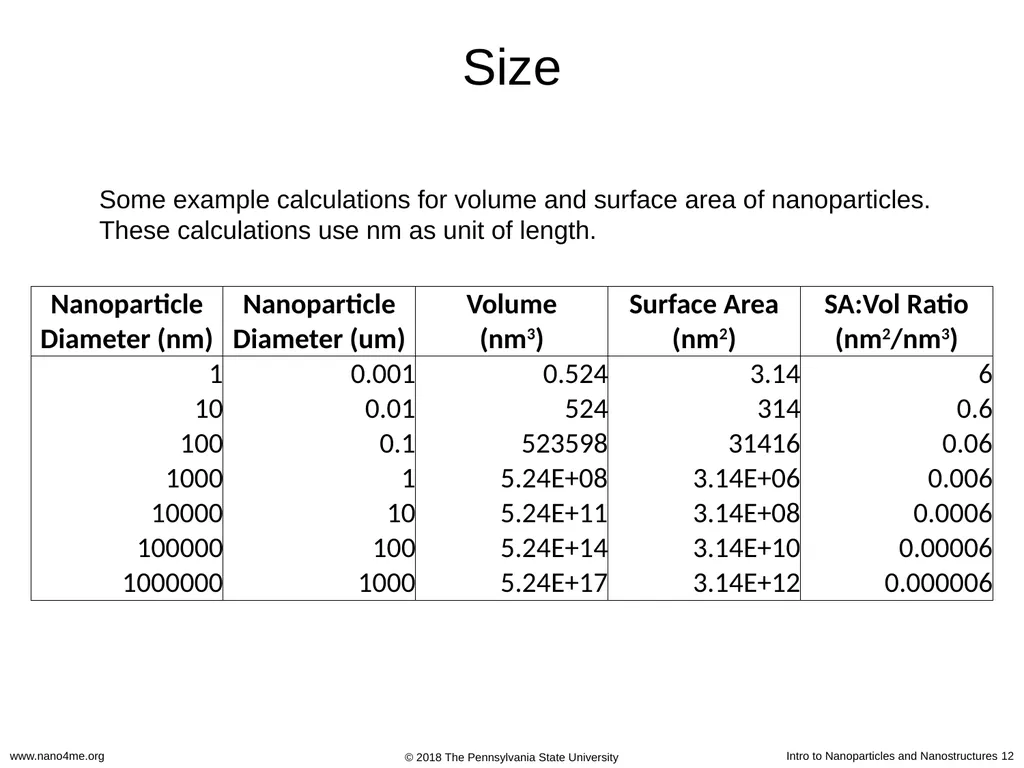
slide12. Size Some example calculations for volume and surface area of nanoparticles.
These calculations use nm as unit of length.<br>
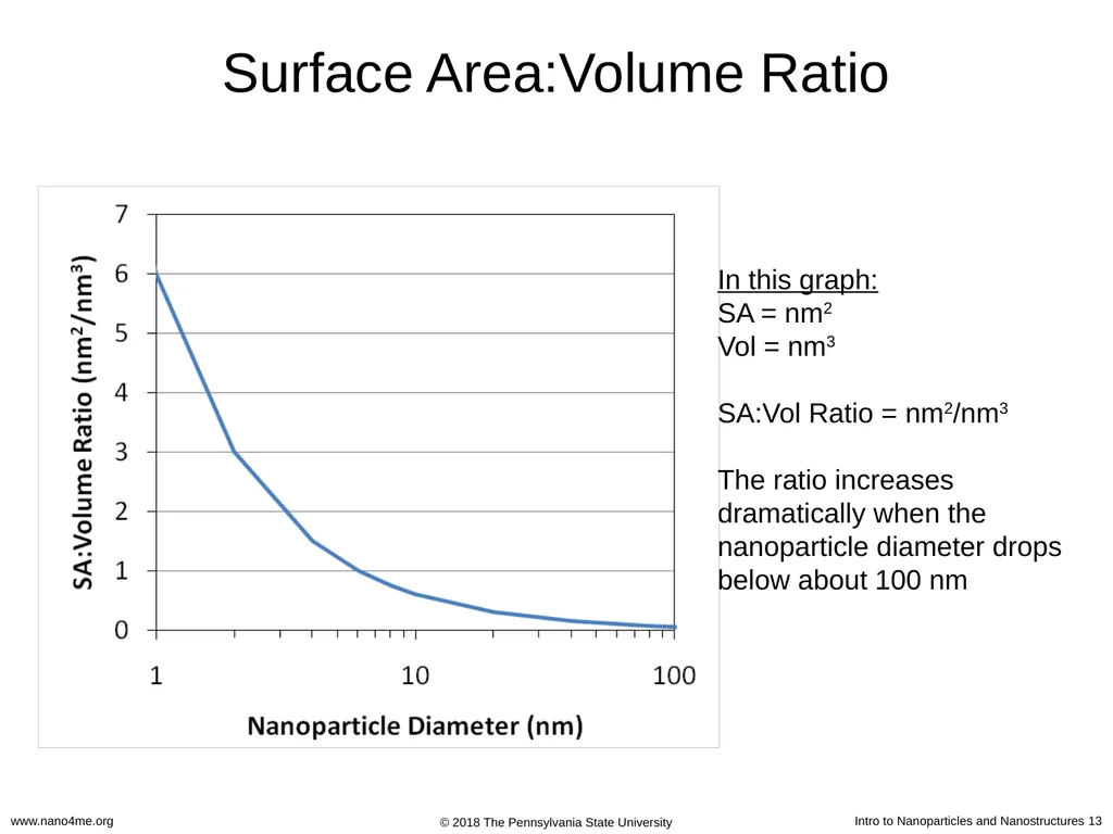
slide13. Surface Area:Volume Ratio In this graph:
SA = nm2
Vol = nm3
SA:Vol Ratio = nm2/nm3
The ratio increases dramatically when the nanoparticle diameter drops below about 100 nm<br>
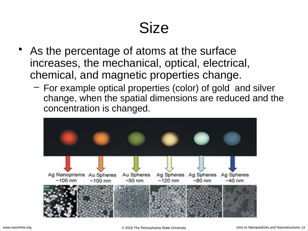
slide14. Size As the percentage of atoms at the surface increases, the mechanical, optical, electrical, chemical, and magnetic properties change.
For example optical properties (color) of gold and silver change, when the spatial dimensions are reduced and the concentration is changed.<br>
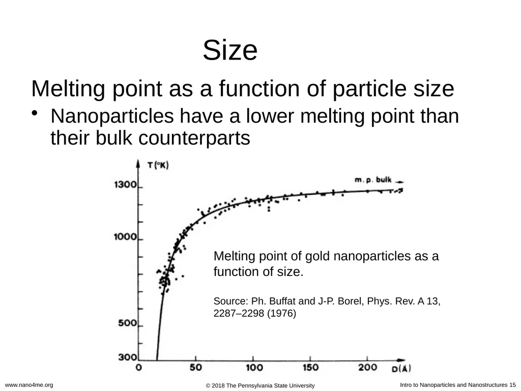
slide15. Size Melting point as a function of particle size
Nanoparticles have a lower melting point than their bulk counterparts Melting point of gold nanoparticles as a function of size.
Source: Ph. Buffat and J-P. Borel, Phys. Rev. A 13, 2287–2298 (1976)<br>
slide16. mp versus Shape Particles: May sinter together at lower than expected temperature.
Rods: Can melt and form spherical droplets if heated too high.
Films: Thin films can form pin-holes. Continued heating can lead to de-wetting behavior and island formation.<br>
slide17. Crystal Structure Most solids are crystalline with their atoms arranged in a regular manner.
This arrangement of atoms impacts the functionality of the material.
Some solids have this order presented over a long range as in a crystal.
Amorphous materials such as glass and wax lack long range order, but they can have a limited short range order, defined as the local environment that each atom experiences. Poole, C., Owens, F. Introduction to Nanotechnology. Wiley, New Jersey. 2003<br>
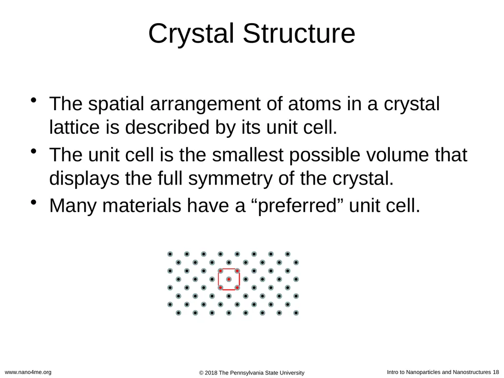
slide18. Crystal Structure The spatial arrangement of atoms in a crystal lattice is described by its unit cell.
The unit cell is the smallest possible volume that displays the full symmetry of the crystal.
Many materials have a “preferred” unit cell.<br>
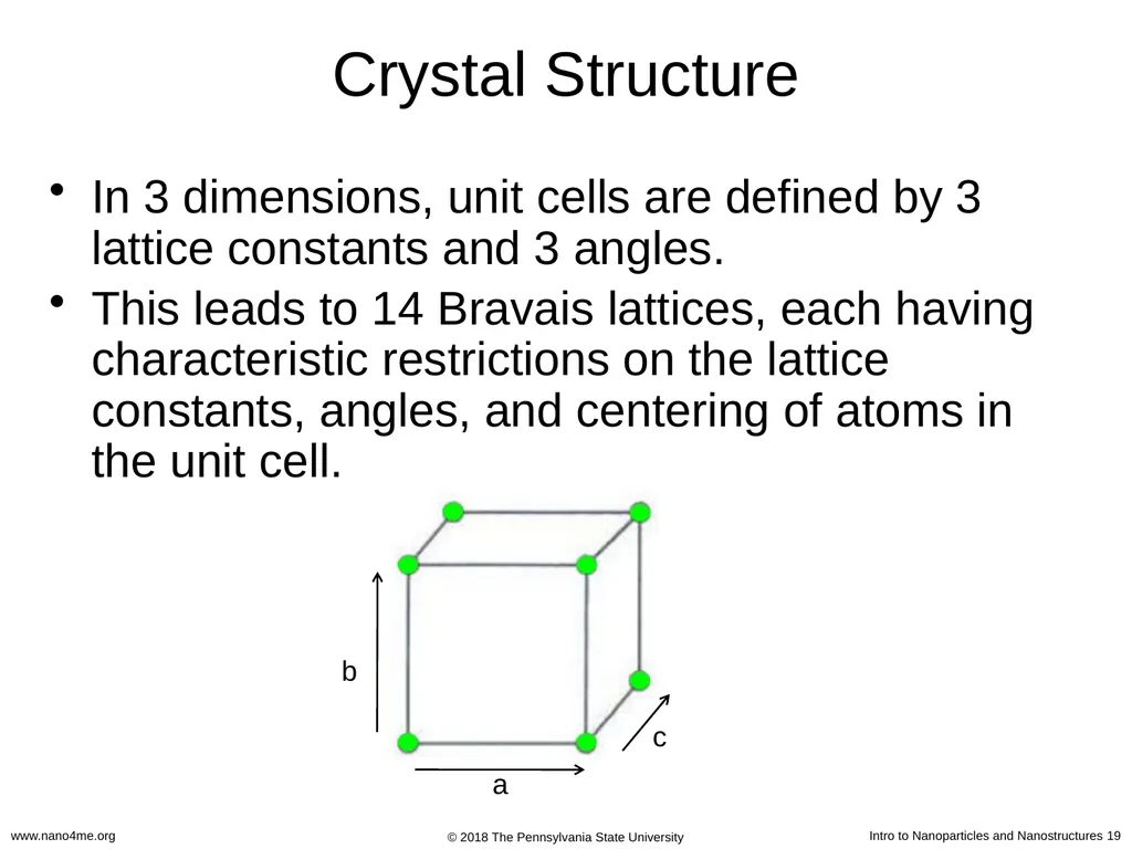
slide19. Crystal Structure In 3 dimensions, unit cells are defined by 3 lattice constants and 3 angles.
This leads to 14 Bravais lattices, each having characteristic restrictions on the lattice constants, angles, and centering of atoms in the unit cell.<br>
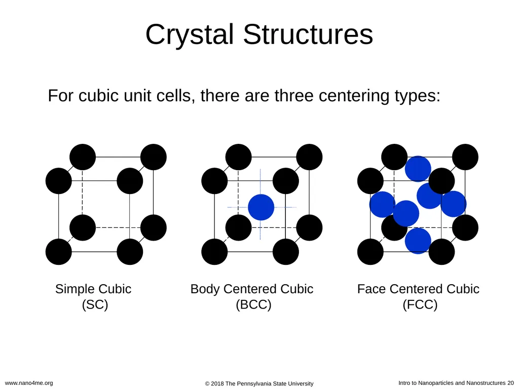
slide20. Crystal Structures Simple Cubic
(SC) Body Centered Cubic
(BCC) Face Centered Cubic
(FCC) For cubic unit cells, there are three centering types:<br>
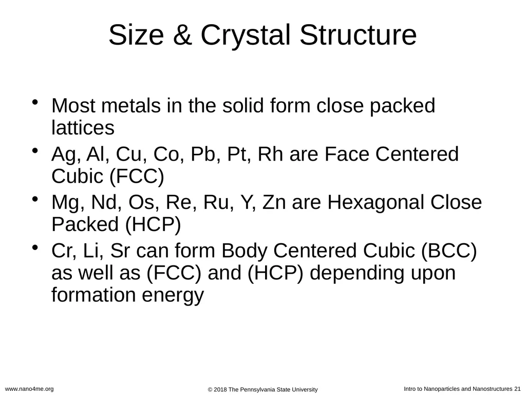
slide21. Size & Crystal Structure Most metals in the solid form close packed lattices
Ag, Al, Cu, Co, Pb, Pt, Rh are Face Centered Cubic (FCC)
Mg, Nd, Os, Re, Ru, Y, Zn are Hexagonal Close Packed (HCP)
Cr, Li, Sr can form Body Centered Cubic (BCC) as well as (FCC) and (HCP) depending upon formation energy<br>
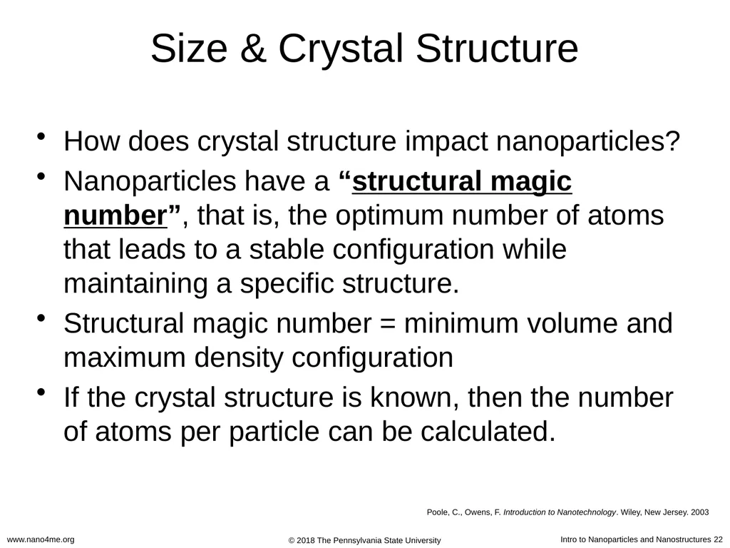
slide22. Size & Crystal Structure How does crystal structure impact nanoparticles?
Nanoparticles have a “structural magic number”, that is, the optimum number of atoms that leads to a stable configuration while maintaining a specific structure.
Structural magic number = minimum volume and maximum density configuration
If the crystal structure is known, then the number of atoms per particle can be calculated. Poole, C., Owens, F. Introduction to Nanotechnology. Wiley, New Jersey. 2003<br>
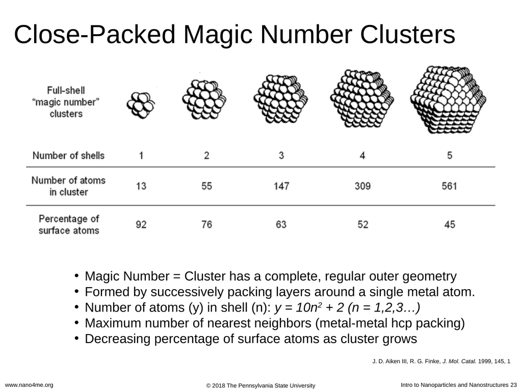
slide23. Close-Packed Magic Number Clusters J. D. Aiken III, R. G. Finke, J. Mol. Catal. 1999, 145, 1 Magic Number = Cluster has a complete, regular outer geometry
Formed by successively packing layers around a single metal atom.
Number of atoms (y) in shell (n): y = 10n2 + 2 (n = 1,2,3…)
Maximum number of nearest neighbors (metal-metal hcp packing)
Decreasing percentage of surface atoms as cluster grows<br>
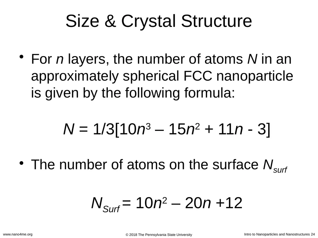
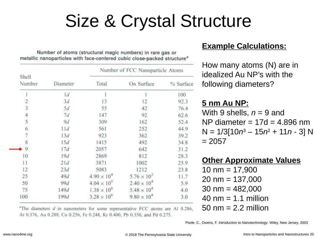
slide24. Size & Crystal Structure For n layers, the number of atoms N in an approximately spherical FCC nanoparticle is given by the following formula:
N = 1/3[10n3 – 15n2 + 11n - 3]
The number of atoms on the surface Nsurf
NSurf = 10n2 – 20n +12<br>
slide25. Size & Crystal Structure Poole, C., Owens, F. Introduction to Nanotechnology. Wiley, New Jersey. 2003 Example Calculations:
How many atoms (N) are in idealized Au NP’s with the following diameters?
5 nm Au NP:
With 9 shells, n = 9 and
NP diameter = 17d = 4.896 nm
N = 1/3[10n3 – 15n2 + 11n - 3] N = 2057
Other Approximate Values
10 nm = 17,900
20 nm = 137,000
30 nm = 482,000
40 nm = 1.1 million
50 nm = 2.2 million<br>
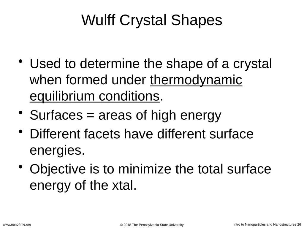
slide26. Wulff Crystal Shapes Used to determine the shape of a crystal when formed under thermodynamic equilibrium conditions.
Surfaces = areas of high energy
Different facets have different surface energies.
Objective is to minimize the total surface energy of the xtal.<br>
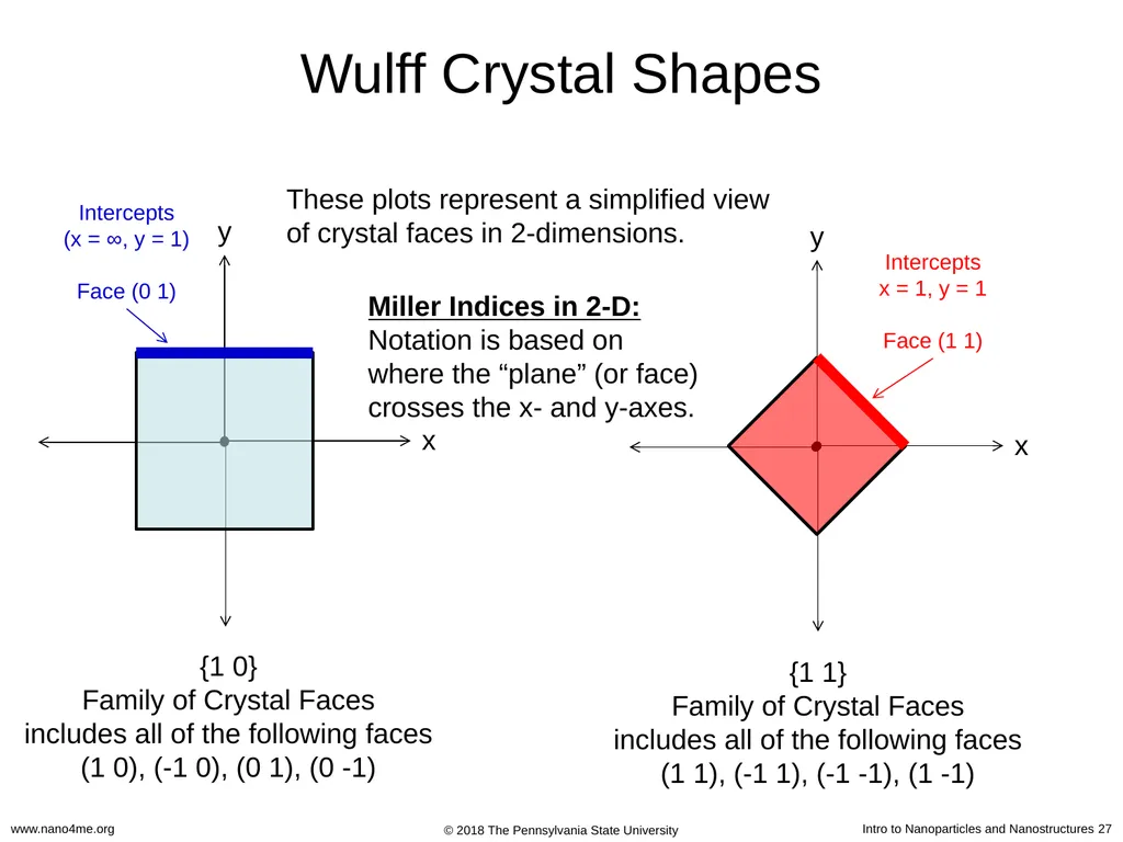
slide27. Wulff Crystal Shapes {1 0}
Family of Crystal Faces
includes all of the following faces
(1 0), (-1 0), (0 1), (0 -1) {1 1}
Family of Crystal Faces
includes all of the following faces
(1 1), (-1 1), (-1 -1), (1 -1) Miller Indices in 2-D:
Notation is based on where the “plane” (or face) crosses the x- and y-axes. Intercepts
(x = ∞, y = 1)
Face (0 1) Intercepts
x = 1, y = 1
Face (1 1) These plots represent a simplified view of crystal faces in 2-dimensions.<br>
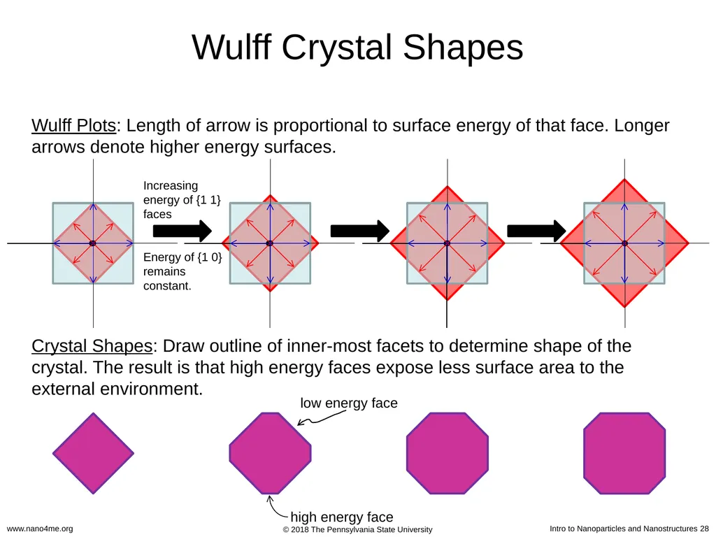
slide28. Wulff Crystal Shapes Crystal Shapes: Draw outline of inner-most facets to determine shape of the crystal. The result is that high energy faces expose less surface area to the external environment. Wulff Plots: Length of arrow is proportional to surface energy of that face. Longer arrows denote higher energy surfaces. high energy face low energy face Increasing energy of {1 1} faces
Energy of {1 0} remains constant.<br>
slide29. Deviations from Ideal Crystals Often, nanoparticles (nanocrystals) do not form well-defined crystal facets.
The Wulff crystal shapes are idealized cases where the crystal surface energies determine the shape (thermodynamic control).
Kinetic factors often play a major role in crystal growth. This explains why different processing conditions can lead to different morphologies for the same material.
Roughening Temperature: Above this temperature, surface atoms on a growing crystal have increased mobility (liquid-like surface) and well-defined facets do not form.
At elevated temps, all faces tend to have similar energy (e.g., on macroscale consider the C-Z process for Si).<br>
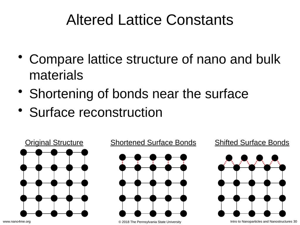
slide30. Altered Lattice Constants Compare lattice structure of nano and bulk materials
Shortening of bonds near the surface
Surface reconstruction Original Structure Shortened Surface Bonds Shifted Surface Bonds<br>
slide31. Mechanical Strength Calculated values for mechanical strength of idealized xtals = 100 to 1000X than experimental
Differentiate between wires and nanocomposites
Transition to higher strength occurs at about 10 microns (above the nanoscale)
2 possible reasons:
Lower number of defects inside the nanowire
Fewer surface defects<br>
slide32. Outline Definition and Examples
Physical Properties
Optical Properties
Surface Plasmons
Quantum Confinement
Electrical Properties
Health Concerns<br>
slide33. Optical Properties The size dependence on the optical properties of nanoparticles is the result of two distinct phenomena:
Surface plasmon resonance for metals
Increased energy level spacing due to the confinement of delocalized energy states. Most prominent in semiconductors Poole, C., Owens, F. Introduction to Nanotechnology. Wiley, New Jersey. 2003<br>
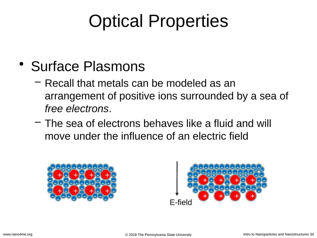
slide34. Optical Properties Surface Plasmons
Recall that metals can be modeled as an arrangement of positive ions surrounded by a sea of free electrons.
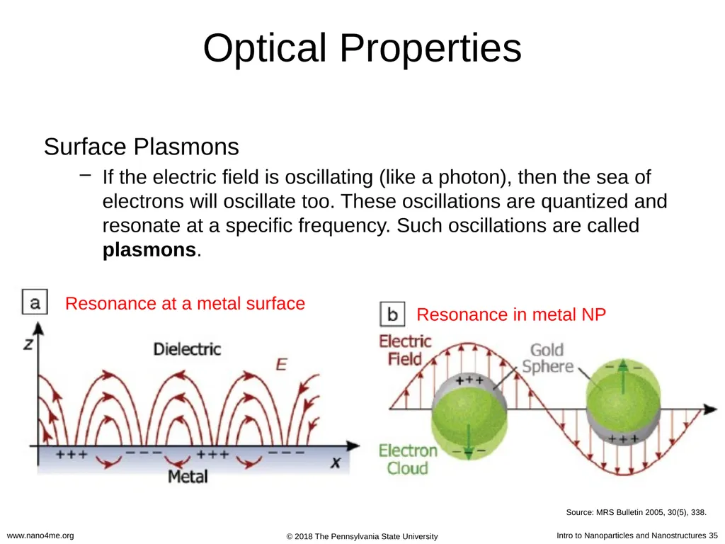
The sea of electrons behaves like a fluid and will move under the influence of an electric field + - + + + + + + + - - - - - - - - - - - - - - - - - - - - - - - - - - - - - - - - - - - - - - - - - - - - - - - - - - - - - - - - - - + - + + + + + + + - - - - - - - - - - - - - - - - - - - - - - - - - - - - - - - - - - - - - - - - - - - - - - - - - - - - - - - - - - - - - - - E-field<br>
slide35. Optical Properties Surface Plasmons
If the electric field is oscillating (like a photon), then the sea of electrons will oscillate too. These oscillations are quantized and resonate at a specific frequency. Such oscillations are called plasmons. Source: MRS Bulletin 2005, 30(5), 338. Resonance at a metal surface Resonance in metal NP<br>
slide36. Optical Properties Surface Plasmons
Formal definition: Plasmons are the coherent excitation of free electrons in a metal.
The plasmon resonance frequency (f) depends on particle size, shape, and material type. It is related to the plasmon energy (E) by Planck’s constant. E=h*f
Surface plasmons are confined to the surface of the material.
The optical properties of metal nanoparticles are dominated by the interaction of surface plasmons with incident photons.<br>
slide37. Optical Properties Surface Plasmons
Metal nanoparticles like gold and silver have plasmon frequencies in the visible range.
When white light impinges on metal nanoparticles the wavelength corresponding to the plasmon frequency is absorbed.
The spectral locations, strengths, and number of plasmon resonances for a given particle depend on the particle’s shape and size.<br>
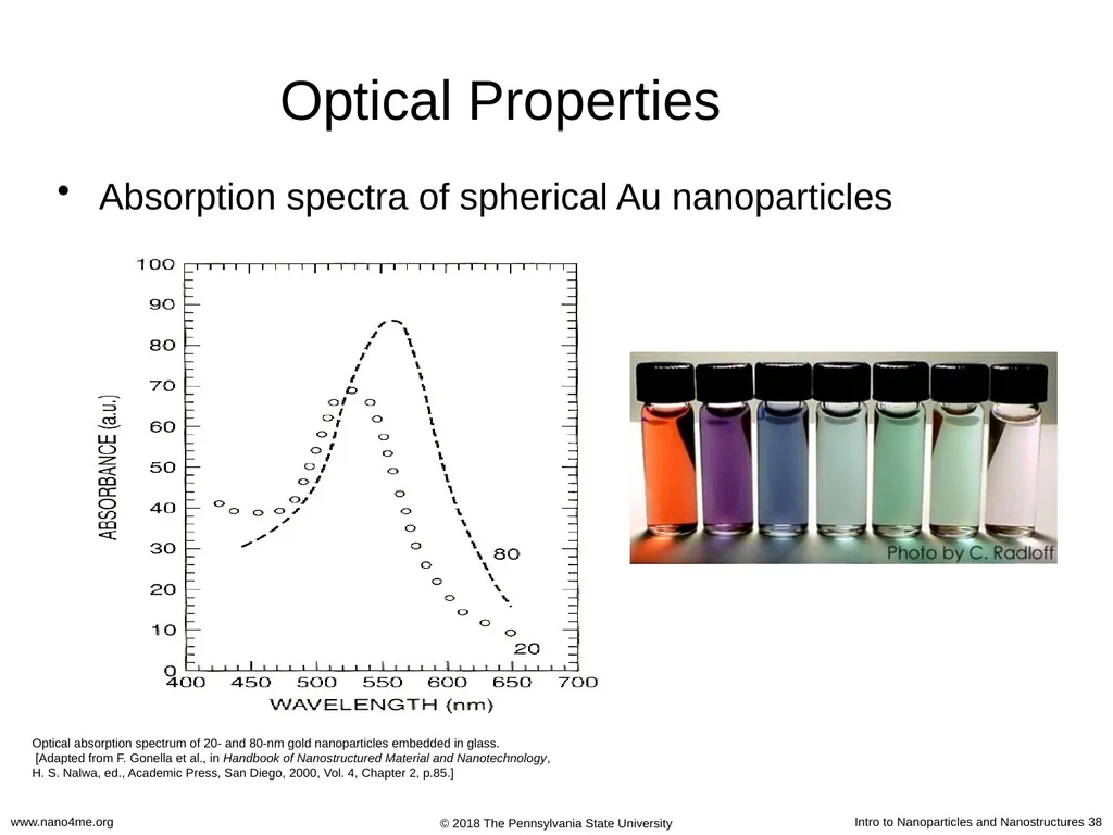
slide38. Optical Properties Optical absorption spectrum of 20- and 80-nm gold nanoparticles embedded in glass.
[Adapted from F. Gonella et al., in Handbook of Nanostructured Material and Nanotechnology,
H. S. Nalwa, ed., Academic Press, San Diego, 2000, Vol. 4, Chapter 2, p.85.] Absorption spectra of spherical Au nanoparticles<br>
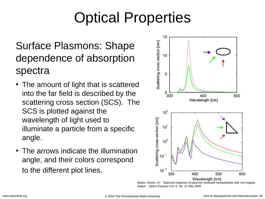
slide39. Optical Properties Martin, Olivier J.F. “Spectral response of plasmon resonant nanoparticles with non-regular shape”. Optics Express Col. 6. No. 11 May 2000 Surface Plasmons: Shape dependence of absorption spectra
The amount of light that is scattered into the far field is described by the scattering cross section (SCS). The SCS is plotted against the wavelength of light used to illuminate a particle from a specific angle.
The arrows indicate the illumination angle, and their colors correspond to the different plot lines.<br>
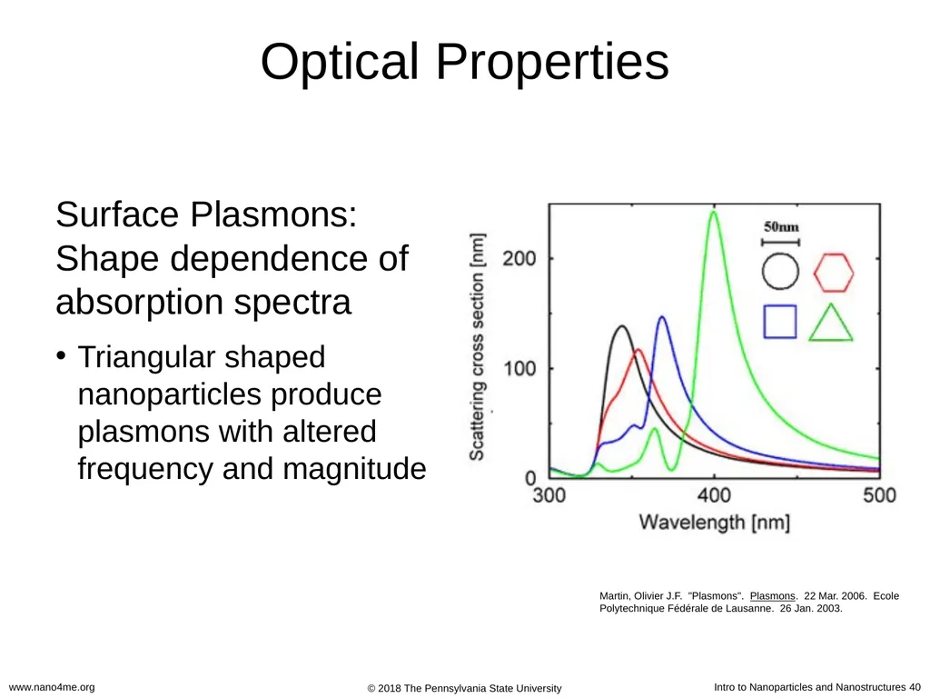
slide40. Optical Properties Martin, Olivier J.F. "Plasmons". Plasmons. 22 Mar. 2006. Ecole Polytechnique Fédérale de Lausanne. 26 Jan. 2003. Surface Plasmons: Shape dependence of absorption spectra
Triangular shaped nanoparticles produce plasmons with altered frequency and magnitude<br>
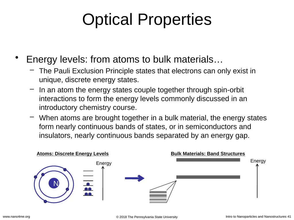
slide41. Optical Properties Energy levels: from atoms to bulk materials…
The Pauli Exclusion Principle states that electrons can only exist in unique, discrete energy states.
In an atom the energy states couple together through spin-orbit interactions to form the energy levels commonly discussed in an introductory chemistry course.
When atoms are brought together in a bulk material, the energy states form nearly continuous bands of states, or in semiconductors and insulators, nearly continuous bands separated by an energy gap.<br>
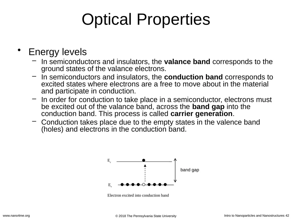
slide42. Optical Properties Energy levels
In semiconductors and insulators, the valance band corresponds to the ground states of the valance electrons.
In semiconductors and insulators, the conduction band corresponds to excited states where electrons are a free to move about in the material and participate in conduction.
In order for conduction to take place in a semiconductor, electrons must be excited out of the valance band, across the band gap into the conduction band. This process is called carrier generation.
Conduction takes place due to the empty states in the valence band (holes) and electrons in the conduction band. band gap<br>
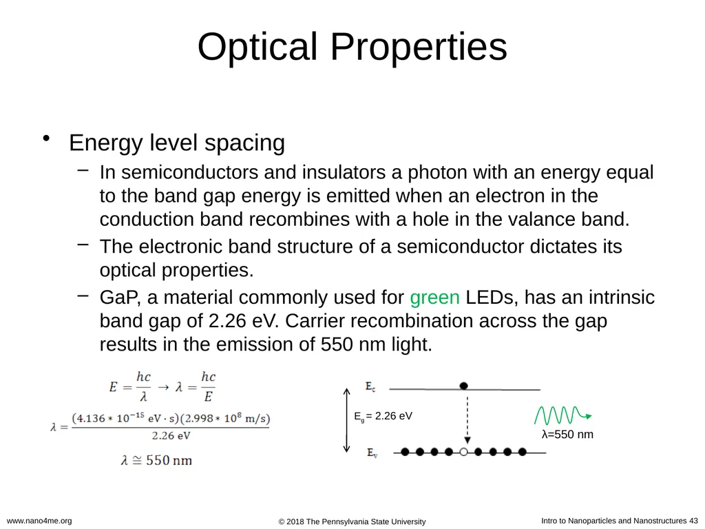
slide43. Optical Properties Energy level spacing
In semiconductors and insulators a photon with an energy equal to the band gap energy is emitted when an electron in the conduction band recombines with a hole in the valance band.
The electronic band structure of a semiconductor dictates its optical properties.
GaP, a material commonly used for green LEDs, has an intrinsic band gap of 2.26 eV. Carrier recombination across the gap results in the emission of 550 nm light. Eg = 2.26 eV λ=550 nm<br>
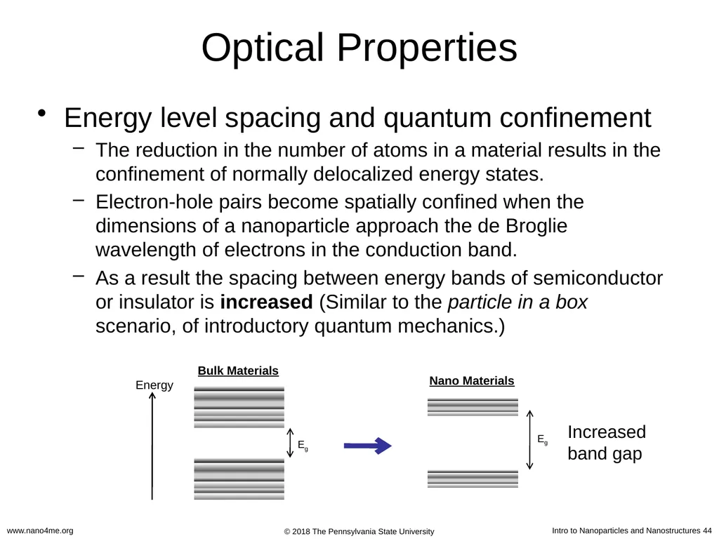
slide44. Optical Properties Energy level spacing and quantum confinement
The reduction in the number of atoms in a material results in the confinement of normally delocalized energy states.
Electron-hole pairs become spatially confined when the dimensions of a nanoparticle approach the de Broglie wavelength of electrons in the conduction band.
As a result the spacing between energy bands of semiconductor or insulator is increased (Similar to the particle in a box scenario, of introductory quantum mechanics.) Increased band gap<br>
slide45. Optical Properties Energy level spacing and quantum confinement
Semiconductor nanoparticles that exhibit 3 dimensional confinement in their electronic band structure are called quantum dots.
What does this all mean?
Quantum dots are band gap tunable.
We can engineer their optical properties by controlling their size.
For this reason quantum dots are highly desirable for biological tagging.<br>
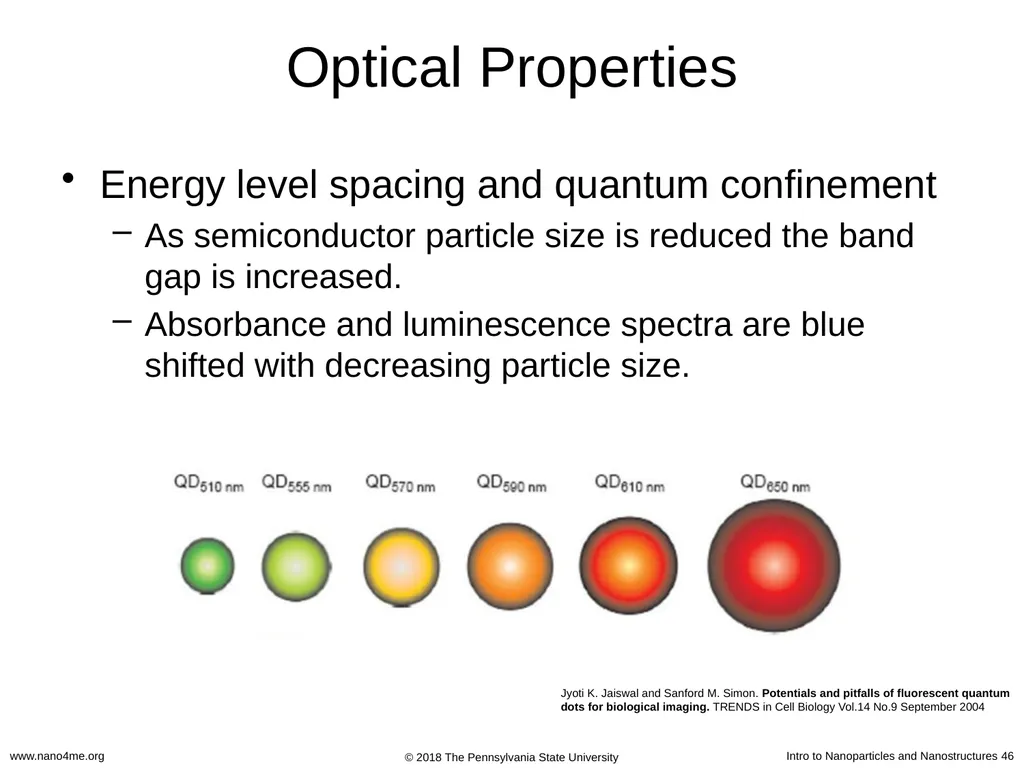
slide46. Optical Properties Energy level spacing and quantum confinement
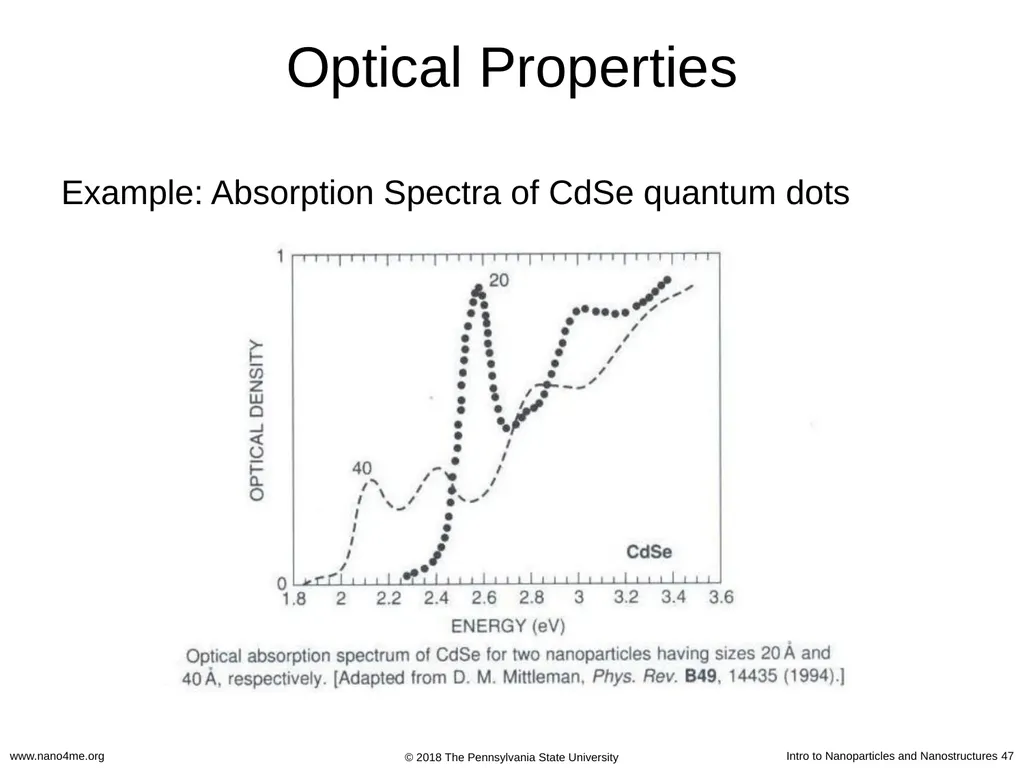
As semiconductor particle size is reduced the band gap is increased.
Absorbance and luminescence spectra are blue shifted with decreasing particle size. CdSe quantum dots Jyoti K. Jaiswal and Sanford M. Simon. Potentials and pitfalls of fluorescent quantum
dots for biological imaging. TRENDS in Cell Biology Vol.14 No.9 September 2004<br>
slide47. Optical Properties Example: Absorption Spectra of CdSe quantum dots<br>
slide48. Outline Definition and Examples
Physical Properties
Optical Properties
Electrical Properties
Health Concerns<br>
slide49. Electrical Properties Effect of structure on conduction
If nanostructures have fewer defects, one would expect increased conductivity vs macroscale
Other electrical effects on the nanoscale:
Surface Scattering
Change in Electronic Structure
Ballistic Conduction
Discrete Charging
Tunneling Conduction
Microstructural Effects<br>
slide50. Surface Scattering Electrons have a mean-free-path (MFP) in solid state materials.
MFP is the distance between scattering events as charge carriers move through the material.
In metals, the MFP is on the order of 10’s of nanometers.
If the dimensions of a nanostructure are smaller than the electron MFP, then surface scattering becomes a factor.<br>
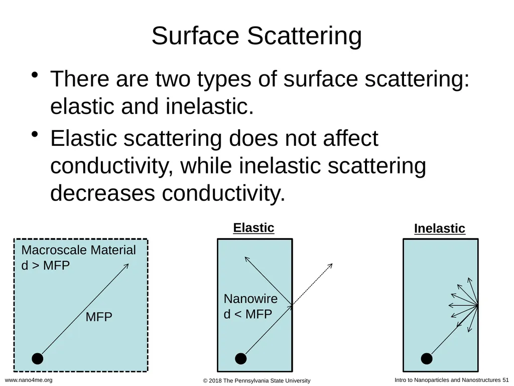
slide51. Surface Scattering There are two types of surface scattering: elastic and inelastic.
Elastic scattering does not affect conductivity, while inelastic scattering decreases conductivity.<br>
slide52. Outline Definition and Examples
Physical Properties
Optical Properties
Electrical Properties
Health Concerns<br>
slide53. Potential Health Concerns Cause for concern:
Nanoparticles are similar in size to many biological structures easily absorbed by the body.
Nanoparticles remain suspended in the environment for extended periods of time.
Health Impacts of nanoparticles are expected to be dependant on composition and structure.<br>
slide54. Potential Health Concerns The potential health concerns of nanomaterials are largely unknown.
The EPA has started the National Nanotechnology Initiative which is providing funding to further investigate this issue.<br>
slide2. Outline Definition and Examples
Physical Properties
Size
Crystal Structure
Melting Point
Mechanical Strength
Optical Properties
Surface Plasmons
Quantum Confinement Effects
Electrical Properties
Health Concerns<br>
slide3. Definition of Nanoparticle A structure with at least 1 dimension less than 1 µm.
Examples:
Sphere-like particles
Ag nanoparticles, buckyballs
Rod-like particles
Si & Ni nanowires
Tube-like particles
Carbon nanotubes
TiO2 nanotubes<br>
slide4. Size is a Material Property? The gold we know:
Material properties don’t change with size
- resistivity
- melting point
- optical absorption The gold we are discovering:
Material properties (such as optical
Absorption, shown here) change with the size of the gold nanoparticle.<br>
slide5. Outline Definition and Examples
Physical Properties
Size
Crystal Structure
Melting Point
Mechanical Strength
Optical Properties
Electrical Properties
Health Concerns<br>
slide6. Unique Characteristics of Nanoparticles Large surface to volume ratio
High percentage of atoms/molecules on the surface
Surface forces are very important, while bulk forces are not as important.
Metal nanoparticles have unique light scattering properties and exhibit plasmon resonance.
Semiconductor nanoparticles may exhibit confined energy states in their electronic band structure (e.g., quantum dots)
Can have unique chemical and physical properties
Same size scale as many biological structures<br>
slide7. Examples of Unusual Properties Lowered phase transition temps
Increased mechanical strength
Different optical properties
Altered electrical conductivity
Magnetic properties
Self-purification and self-perfection<br>
slide8. Physical Properties of Nanoparticles Physical properties of nanoparticles are dependent on:
Size
Shape (spheres, rods, platelets, etc.)
Composition
Crystal Structure (FCC, BCC, etc.)
Surface ligands or capping agents
The medium in which they are dispersed<br>
slide9. Size Molecules, nanoparticles, and bulk materials can be distinguished by the number of atoms comprising each type of material.
Note: these are very approximate numbers! Poole, C., Owens, F. Introduction to Nanotechnology. Wiley, New Jersey. 2003 1 10 102 103 104 105 106 Molecules Nanoparticles Bulk # of atoms<br>
slide10. Size Nanoparticles exhibit unique properties due to their high surface area to volume ratio.
A spherical particle has a diameter (D) of 100nm.
Calculate the volume (V) and surface area (SA) Poole, C., Owens, F. Introduction to Nanotechnology. Wiley, New Jersey. 2003<br>
slide11. Surface Area:Volume Ratio This gives an approximate surface area to volume ratio of >107:1 which is significantly larger than a macro sized particle.
As the surface area to volume ratio increases so does the percentage of atoms at the surface and surface forces become more dominant.
Generally accepted material properties are derived from the bulk, where the percentage of atoms at the surface is miniscule. These properties change at the nanoscale.<br>
slide12. Size Some example calculations for volume and surface area of nanoparticles.
These calculations use nm as unit of length.<br>
slide13. Surface Area:Volume Ratio In this graph:
SA = nm2
Vol = nm3
SA:Vol Ratio = nm2/nm3
The ratio increases dramatically when the nanoparticle diameter drops below about 100 nm<br>
slide14. Size As the percentage of atoms at the surface increases, the mechanical, optical, electrical, chemical, and magnetic properties change.
For example optical properties (color) of gold and silver change, when the spatial dimensions are reduced and the concentration is changed.<br>
slide15. Size Melting point as a function of particle size
Nanoparticles have a lower melting point than their bulk counterparts Melting point of gold nanoparticles as a function of size.
Source: Ph. Buffat and J-P. Borel, Phys. Rev. A 13, 2287–2298 (1976)<br>
slide16. mp versus Shape Particles: May sinter together at lower than expected temperature.
Rods: Can melt and form spherical droplets if heated too high.
Films: Thin films can form pin-holes. Continued heating can lead to de-wetting behavior and island formation.<br>
slide17. Crystal Structure Most solids are crystalline with their atoms arranged in a regular manner.
This arrangement of atoms impacts the functionality of the material.
Some solids have this order presented over a long range as in a crystal.
Amorphous materials such as glass and wax lack long range order, but they can have a limited short range order, defined as the local environment that each atom experiences. Poole, C., Owens, F. Introduction to Nanotechnology. Wiley, New Jersey. 2003<br>
slide18. Crystal Structure The spatial arrangement of atoms in a crystal lattice is described by its unit cell.
The unit cell is the smallest possible volume that displays the full symmetry of the crystal.
Many materials have a “preferred” unit cell.<br>
slide19. Crystal Structure In 3 dimensions, unit cells are defined by 3 lattice constants and 3 angles.
This leads to 14 Bravais lattices, each having characteristic restrictions on the lattice constants, angles, and centering of atoms in the unit cell.<br>
slide20. Crystal Structures Simple Cubic
(SC) Body Centered Cubic
(BCC) Face Centered Cubic
(FCC) For cubic unit cells, there are three centering types:<br>
slide21. Size & Crystal Structure Most metals in the solid form close packed lattices
Ag, Al, Cu, Co, Pb, Pt, Rh are Face Centered Cubic (FCC)
Mg, Nd, Os, Re, Ru, Y, Zn are Hexagonal Close Packed (HCP)
Cr, Li, Sr can form Body Centered Cubic (BCC) as well as (FCC) and (HCP) depending upon formation energy<br>
slide22. Size & Crystal Structure How does crystal structure impact nanoparticles?
Nanoparticles have a “structural magic number”, that is, the optimum number of atoms that leads to a stable configuration while maintaining a specific structure.
Structural magic number = minimum volume and maximum density configuration
If the crystal structure is known, then the number of atoms per particle can be calculated. Poole, C., Owens, F. Introduction to Nanotechnology. Wiley, New Jersey. 2003<br>
slide23. Close-Packed Magic Number Clusters J. D. Aiken III, R. G. Finke, J. Mol. Catal. 1999, 145, 1 Magic Number = Cluster has a complete, regular outer geometry
Formed by successively packing layers around a single metal atom.
Number of atoms (y) in shell (n): y = 10n2 + 2 (n = 1,2,3…)
Maximum number of nearest neighbors (metal-metal hcp packing)
Decreasing percentage of surface atoms as cluster grows<br>
slide24. Size & Crystal Structure For n layers, the number of atoms N in an approximately spherical FCC nanoparticle is given by the following formula:
N = 1/3[10n3 – 15n2 + 11n - 3]
The number of atoms on the surface Nsurf
NSurf = 10n2 – 20n +12<br>
slide25. Size & Crystal Structure Poole, C., Owens, F. Introduction to Nanotechnology. Wiley, New Jersey. 2003 Example Calculations:
How many atoms (N) are in idealized Au NP’s with the following diameters?
5 nm Au NP:
With 9 shells, n = 9 and
NP diameter = 17d = 4.896 nm
N = 1/3[10n3 – 15n2 + 11n - 3] N = 2057
Other Approximate Values
10 nm = 17,900
20 nm = 137,000
30 nm = 482,000
40 nm = 1.1 million
50 nm = 2.2 million<br>
slide26. Wulff Crystal Shapes Used to determine the shape of a crystal when formed under thermodynamic equilibrium conditions.
Surfaces = areas of high energy
Different facets have different surface energies.
Objective is to minimize the total surface energy of the xtal.<br>
slide27. Wulff Crystal Shapes {1 0}
Family of Crystal Faces
includes all of the following faces
(1 0), (-1 0), (0 1), (0 -1) {1 1}
Family of Crystal Faces
includes all of the following faces
(1 1), (-1 1), (-1 -1), (1 -1) Miller Indices in 2-D:
Notation is based on where the “plane” (or face) crosses the x- and y-axes. Intercepts
(x = ∞, y = 1)
Face (0 1) Intercepts
x = 1, y = 1
Face (1 1) These plots represent a simplified view of crystal faces in 2-dimensions.<br>
slide28. Wulff Crystal Shapes Crystal Shapes: Draw outline of inner-most facets to determine shape of the crystal. The result is that high energy faces expose less surface area to the external environment. Wulff Plots: Length of arrow is proportional to surface energy of that face. Longer arrows denote higher energy surfaces. high energy face low energy face Increasing energy of {1 1} faces
Energy of {1 0} remains constant.<br>
slide29. Deviations from Ideal Crystals Often, nanoparticles (nanocrystals) do not form well-defined crystal facets.
The Wulff crystal shapes are idealized cases where the crystal surface energies determine the shape (thermodynamic control).
Kinetic factors often play a major role in crystal growth. This explains why different processing conditions can lead to different morphologies for the same material.
Roughening Temperature: Above this temperature, surface atoms on a growing crystal have increased mobility (liquid-like surface) and well-defined facets do not form.
At elevated temps, all faces tend to have similar energy (e.g., on macroscale consider the C-Z process for Si).<br>
slide30. Altered Lattice Constants Compare lattice structure of nano and bulk materials
Shortening of bonds near the surface
Surface reconstruction Original Structure Shortened Surface Bonds Shifted Surface Bonds<br>
slide31. Mechanical Strength Calculated values for mechanical strength of idealized xtals = 100 to 1000X than experimental
Differentiate between wires and nanocomposites
Transition to higher strength occurs at about 10 microns (above the nanoscale)
2 possible reasons:
Lower number of defects inside the nanowire
Fewer surface defects<br>
slide32. Outline Definition and Examples
Physical Properties
Optical Properties
Surface Plasmons
Quantum Confinement
Electrical Properties
Health Concerns<br>
slide33. Optical Properties The size dependence on the optical properties of nanoparticles is the result of two distinct phenomena:
Surface plasmon resonance for metals
Increased energy level spacing due to the confinement of delocalized energy states. Most prominent in semiconductors Poole, C., Owens, F. Introduction to Nanotechnology. Wiley, New Jersey. 2003<br>
slide34. Optical Properties Surface Plasmons
Recall that metals can be modeled as an arrangement of positive ions surrounded by a sea of free electrons.
The sea of electrons behaves like a fluid and will move under the influence of an electric field + - + + + + + + + - - - - - - - - - - - - - - - - - - - - - - - - - - - - - - - - - - - - - - - - - - - - - - - - - - - - - - - - - - + - + + + + + + + - - - - - - - - - - - - - - - - - - - - - - - - - - - - - - - - - - - - - - - - - - - - - - - - - - - - - - - - - - - - - - - E-field<br>
slide35. Optical Properties Surface Plasmons
If the electric field is oscillating (like a photon), then the sea of electrons will oscillate too. These oscillations are quantized and resonate at a specific frequency. Such oscillations are called plasmons. Source: MRS Bulletin 2005, 30(5), 338. Resonance at a metal surface Resonance in metal NP<br>
slide36. Optical Properties Surface Plasmons
Formal definition: Plasmons are the coherent excitation of free electrons in a metal.
The plasmon resonance frequency (f) depends on particle size, shape, and material type. It is related to the plasmon energy (E) by Planck’s constant. E=h*f
Surface plasmons are confined to the surface of the material.
The optical properties of metal nanoparticles are dominated by the interaction of surface plasmons with incident photons.<br>
slide37. Optical Properties Surface Plasmons
Metal nanoparticles like gold and silver have plasmon frequencies in the visible range.
When white light impinges on metal nanoparticles the wavelength corresponding to the plasmon frequency is absorbed.
The spectral locations, strengths, and number of plasmon resonances for a given particle depend on the particle’s shape and size.<br>
slide38. Optical Properties Optical absorption spectrum of 20- and 80-nm gold nanoparticles embedded in glass.
[Adapted from F. Gonella et al., in Handbook of Nanostructured Material and Nanotechnology,
H. S. Nalwa, ed., Academic Press, San Diego, 2000, Vol. 4, Chapter 2, p.85.] Absorption spectra of spherical Au nanoparticles<br>
slide39. Optical Properties Martin, Olivier J.F. “Spectral response of plasmon resonant nanoparticles with non-regular shape”. Optics Express Col. 6. No. 11 May 2000 Surface Plasmons: Shape dependence of absorption spectra
The amount of light that is scattered into the far field is described by the scattering cross section (SCS). The SCS is plotted against the wavelength of light used to illuminate a particle from a specific angle.
The arrows indicate the illumination angle, and their colors correspond to the different plot lines.<br>
slide40. Optical Properties Martin, Olivier J.F. "Plasmons". Plasmons. 22 Mar. 2006. Ecole Polytechnique Fédérale de Lausanne. 26 Jan. 2003. Surface Plasmons: Shape dependence of absorption spectra
Triangular shaped nanoparticles produce plasmons with altered frequency and magnitude<br>
slide41. Optical Properties Energy levels: from atoms to bulk materials…
The Pauli Exclusion Principle states that electrons can only exist in unique, discrete energy states.
In an atom the energy states couple together through spin-orbit interactions to form the energy levels commonly discussed in an introductory chemistry course.
When atoms are brought together in a bulk material, the energy states form nearly continuous bands of states, or in semiconductors and insulators, nearly continuous bands separated by an energy gap.<br>
slide42. Optical Properties Energy levels
In semiconductors and insulators, the valance band corresponds to the ground states of the valance electrons.
In semiconductors and insulators, the conduction band corresponds to excited states where electrons are a free to move about in the material and participate in conduction.
In order for conduction to take place in a semiconductor, electrons must be excited out of the valance band, across the band gap into the conduction band. This process is called carrier generation.
Conduction takes place due to the empty states in the valence band (holes) and electrons in the conduction band. band gap<br>
slide43. Optical Properties Energy level spacing
In semiconductors and insulators a photon with an energy equal to the band gap energy is emitted when an electron in the conduction band recombines with a hole in the valance band.
The electronic band structure of a semiconductor dictates its optical properties.
GaP, a material commonly used for green LEDs, has an intrinsic band gap of 2.26 eV. Carrier recombination across the gap results in the emission of 550 nm light. Eg = 2.26 eV λ=550 nm<br>
slide44. Optical Properties Energy level spacing and quantum confinement
The reduction in the number of atoms in a material results in the confinement of normally delocalized energy states.
Electron-hole pairs become spatially confined when the dimensions of a nanoparticle approach the de Broglie wavelength of electrons in the conduction band.
As a result the spacing between energy bands of semiconductor or insulator is increased (Similar to the particle in a box scenario, of introductory quantum mechanics.) Increased band gap<br>
slide45. Optical Properties Energy level spacing and quantum confinement
Semiconductor nanoparticles that exhibit 3 dimensional confinement in their electronic band structure are called quantum dots.
What does this all mean?
Quantum dots are band gap tunable.
We can engineer their optical properties by controlling their size.
For this reason quantum dots are highly desirable for biological tagging.<br>
slide46. Optical Properties Energy level spacing and quantum confinement
As semiconductor particle size is reduced the band gap is increased.
Absorbance and luminescence spectra are blue shifted with decreasing particle size. CdSe quantum dots Jyoti K. Jaiswal and Sanford M. Simon. Potentials and pitfalls of fluorescent quantum
dots for biological imaging. TRENDS in Cell Biology Vol.14 No.9 September 2004<br>
slide47. Optical Properties Example: Absorption Spectra of CdSe quantum dots<br>
slide48. Outline Definition and Examples
Physical Properties
Optical Properties
Electrical Properties
Health Concerns<br>
slide49. Electrical Properties Effect of structure on conduction
If nanostructures have fewer defects, one would expect increased conductivity vs macroscale
Other electrical effects on the nanoscale:
Surface Scattering
Change in Electronic Structure
Ballistic Conduction
Discrete Charging
Tunneling Conduction
Microstructural Effects<br>
slide50. Surface Scattering Electrons have a mean-free-path (MFP) in solid state materials.
MFP is the distance between scattering events as charge carriers move through the material.
In metals, the MFP is on the order of 10’s of nanometers.
If the dimensions of a nanostructure are smaller than the electron MFP, then surface scattering becomes a factor.<br>
slide51. Surface Scattering There are two types of surface scattering: elastic and inelastic.
Elastic scattering does not affect conductivity, while inelastic scattering decreases conductivity.<br>
slide52. Outline Definition and Examples
Physical Properties
Optical Properties
Electrical Properties
Health Concerns<br>
slide53. Potential Health Concerns Cause for concern:
Nanoparticles are similar in size to many biological structures easily absorbed by the body.
Nanoparticles remain suspended in the environment for extended periods of time.
Health Impacts of nanoparticles are expected to be dependant on composition and structure.<br>
slide54. Potential Health Concerns The potential health concerns of nanomaterials are largely unknown.
The EPA has started the National Nanotechnology Initiative which is providing funding to further investigate this issue.<br>