02
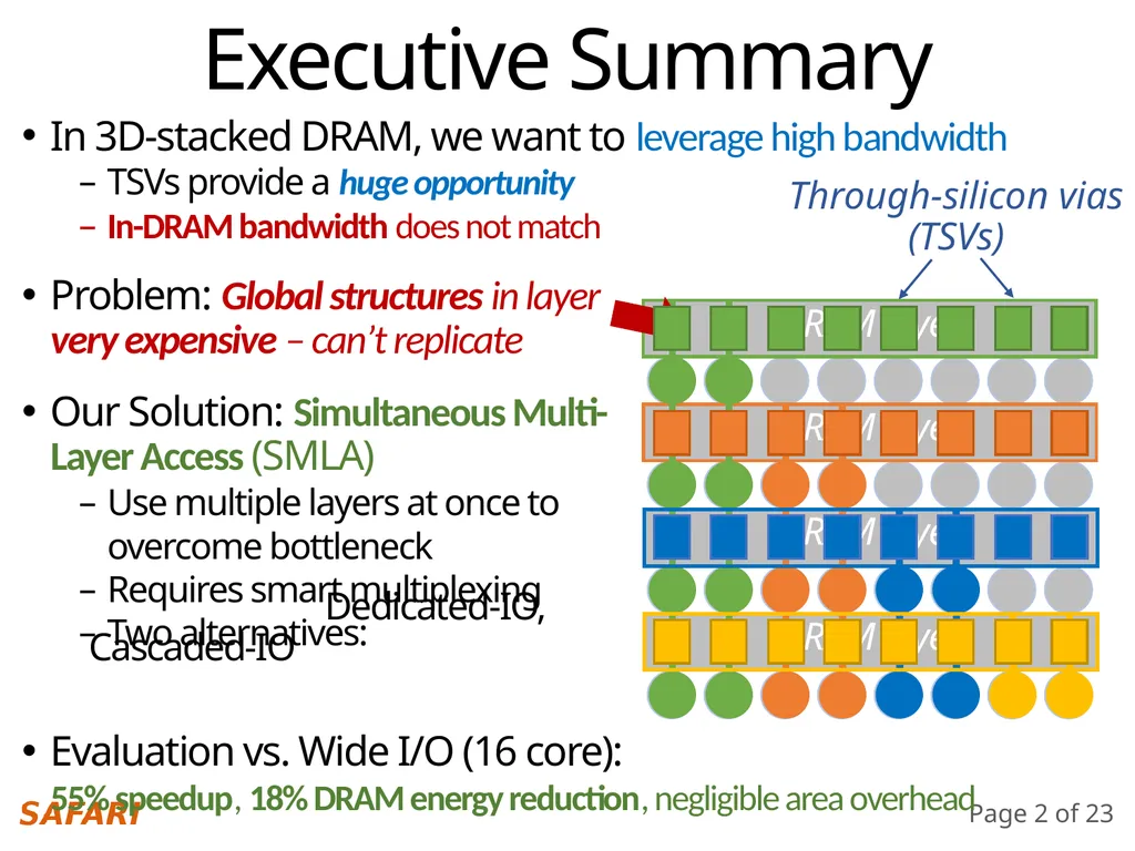
DRAM layer DRAM layer DRAM layer DRAM layer Executive Summary In 3D-stacked DRAM, we want to leverage high bandwidth
TSVs provide a huge opportunity
In-DRAM bandwidth does not match
Problem: Global structures in layer �very expensive – can’t replicate
Our Solution: Simultaneous Multi-�Layer Access (SMLA)
Use multiple layers at once to �overcome bottleneck
Requires smart multiplexing
Two alternatives: �
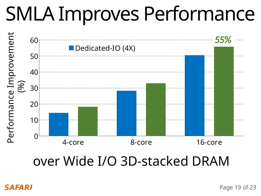
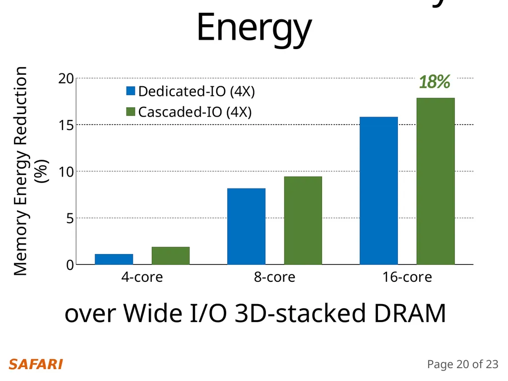
Evaluation vs. Wide I/O (16 core):�55% speedup, 18% DRAM energy reduction, negligible area overhead Through-silicon vias
(TSVs) Dedicated-IO, Cascaded-IO<br>
04
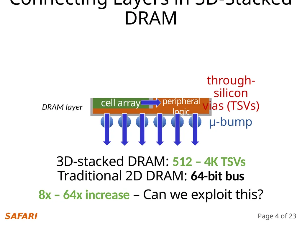
Connecting Layers in 3D-Stacked DRAM DRAM layer μ-bump through-silicon vias (TSVs) 3D-stacked DRAM: 512 – 4K TSVs
Traditional 2D DRAM: 64-bit bus
8x – 64x increase – Can we exploit this?<br>
05
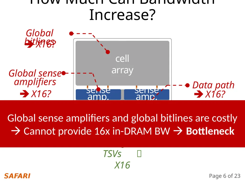
accessed layer If TSVs provide 16x bus width vs. 2D,�do we get 16x bandwidth from the DRAM? How Much Can Bandwidth Increase? Can each layer deliver 16x the data?<br>
06
peripheral
logic bank bank Global sense amplifiers Global bitlines Data path TSVs X16 X16? X16? X16? How Much Can Bandwidth Increase? cell
array Global sense amplifiers and global bitlines are costly
Cannot provide 16x in-DRAM BW Bottleneck<br>
07
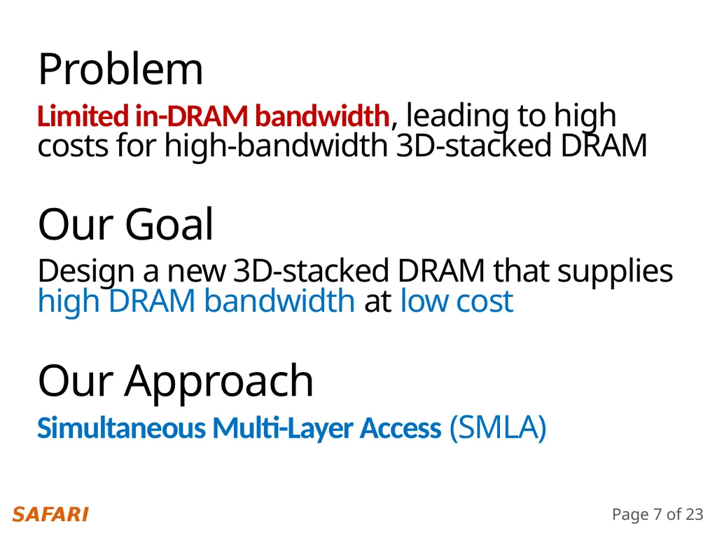
Our Goal
Design a new 3D-stacked DRAM that supplies high DRAM bandwidth at low cost Problem
Limited in-DRAM bandwidth, leading to high costs for high-bandwidth 3D-stacked DRAM Our Approach
Simultaneous Multi-Layer Access (SMLA)<br>
08
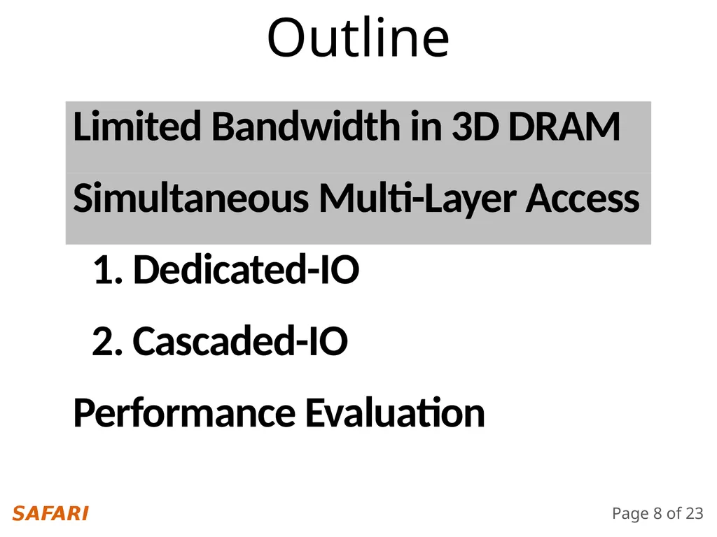
Outline 2. Cascaded-IO Performance Evaluation Limited Bandwidth in 3D DRAM Simultaneous Multi-Layer Access 1. Dedicated-IO Limited Bandwidth in 3D DRAM Simultaneous Multi-Layer Access<br>
09
CHALLENGE: How to avoid TSV channel conflicts? CHALLENGE: How to avoid TSV channel conflicts?
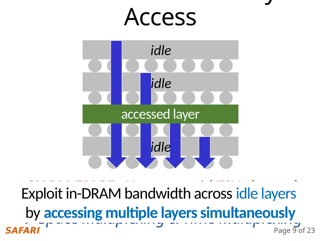
Space Multiplexing & Time Multiplexing Exploit in-DRAM bandwidth across idle layers �by accessing multiple layers simultaneously Simultaneous Multi-Layer Access accessed layer idle idle idle<br>
10
Outline 2. Cascaded-IO Performance Evaluation Limited Bandwidth in 3D DRAM Simultaneous Multi-Layer Access 1. Dedicated-IO Simultaneous Multi-Layer Access 1. Dedicated-IO<br>
11
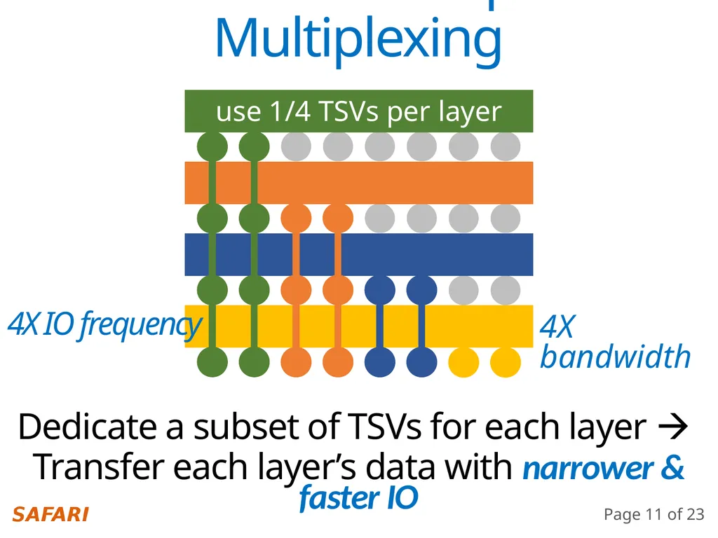
Dedicated-IO: Space Multiplexing Dedicate a subset of TSVs for each layer
Transfer each layer’s data with narrower & faster IO 4X bandwidth 4X IO frequency use 1/4 TSVs per layer<br>
12
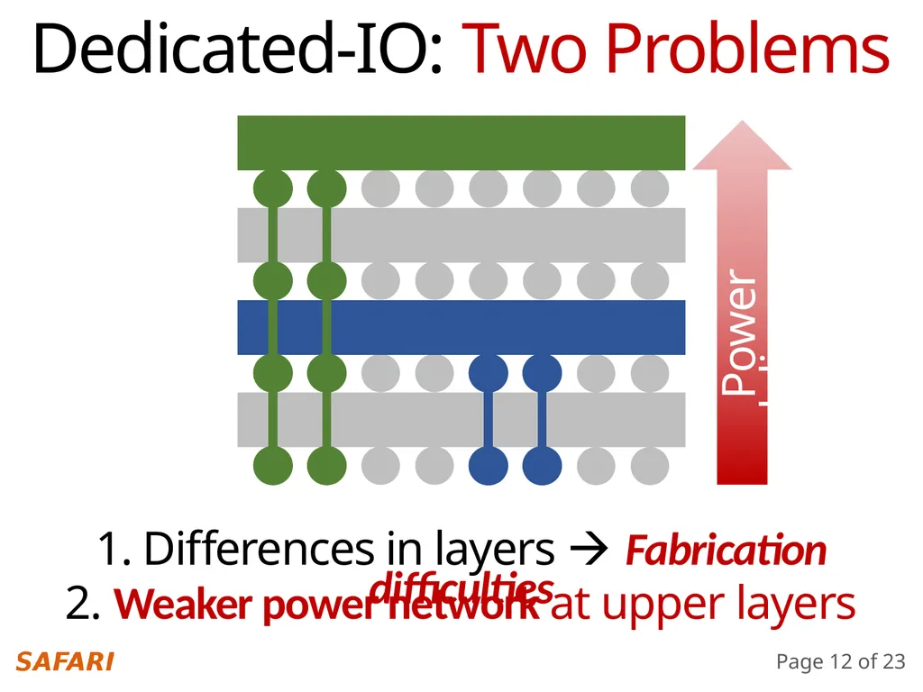
Dedicated-IO: Two Problems 1. Differences in layers Fabrication difficulties Use 1/4 TSVs with 4X IO freq. 2. Weaker power network at upper layers Power delivery<br>
13
2. Cascaded-IO 1. Dedicated-IO Outline 2. Cascaded-IO Performance Evaluation Limited Bandwidth in 3D DRAM Simultaneous Multi-Layer Access 1. Dedicated-IO<br>
14
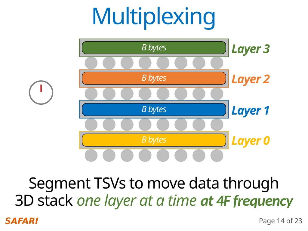
Cascaded-IO: Time Multiplexing Layer 3 Layer 2 Layer 1 Layer 0 Segment TSVs to move data through
3D stack one layer at a time at 4F frequency B bytes B bytes B bytes B bytes<br>
15
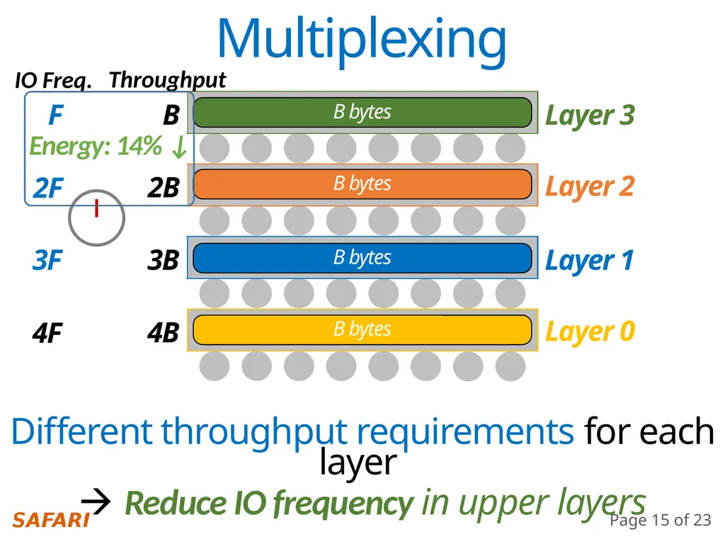
Cascaded-IO: Time Multiplexing Layer 3 Layer 2 Layer 1 Layer 0 B bytes B bytes B bytes B bytes Different throughput requirements for each layer
Reduce IO frequency in upper layers B B B B Throughput 2B 2B 2B 3B 3B 4B IO Freq. F 2F 3F 4F Energy: 14% ↓<br>
16
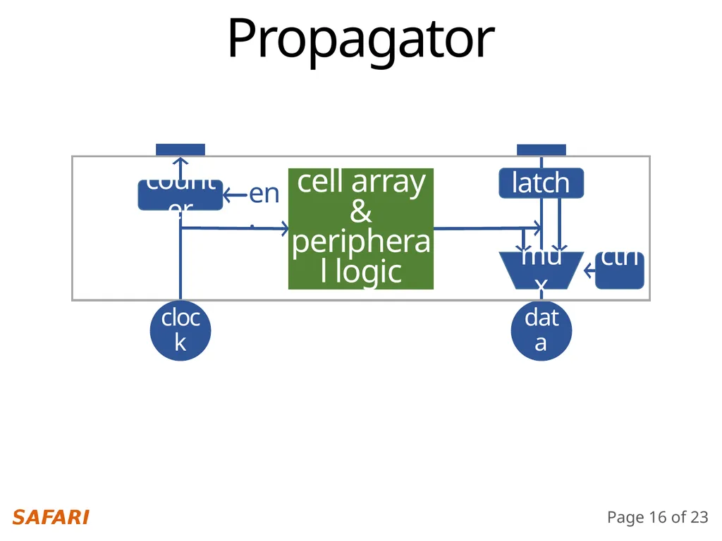
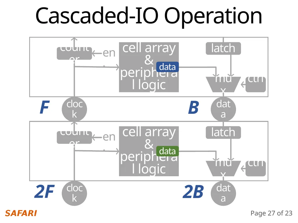
Cascaded-IO Data Multiplexer data latch mux ctrl. counter en. Cascaded-IO Clock Propagator cell array &
peripheral logic<br>
17
Outline 2. Cascaded-IO Performance Evaluation Limited Bandwidth in 3D DRAM Simultaneous Multi-Layer Access 1. Dedicated-IO 2. Cascaded-IO Performance Evaluation<br>
18
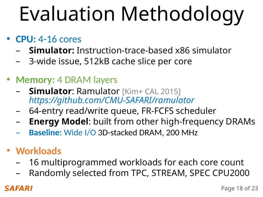
CPU: 4-16 cores
Simulator: Instruction-trace-based x86 simulator
3-wide issue, 512kB cache slice per core
Memory: 4 DRAM layers
Simulator: Ramulator [Kim+ CAL 2015]�https://github.com/CMU-SAFARI/ramulator
64-entry read/write queue, FR-FCFS scheduler
Energy Model: built from other high-frequency DRAMs
Baseline: Wide I/O 3D-stacked DRAM, 200 MHz
Workloads
16 multiprogrammed workloads for each core count
Randomly selected from TPC, STREAM, SPEC CPU2000 Evaluation Methodology<br>
19
SMLA Improves Performance Performance Improvement (%) over Wide I/O 3D-stacked DRAM 55%<br>
20
SMLA Reduces Memory Energy Memory Energy Reduction (%) over Wide I/O 3D-stacked DRAM 18%<br>
21
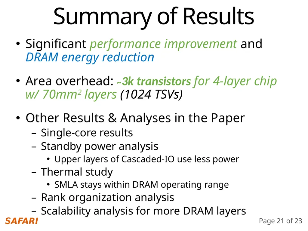
Summary of Results Significant performance improvement and DRAM energy reduction
Area overhead: ~3k transistors for 4-layer chip w/ 70mm2 layers (1024 TSVs)
Other Results & Analyses in the Paper
Single-core results
Standby power analysis
Upper layers of Cascaded-IO use less power
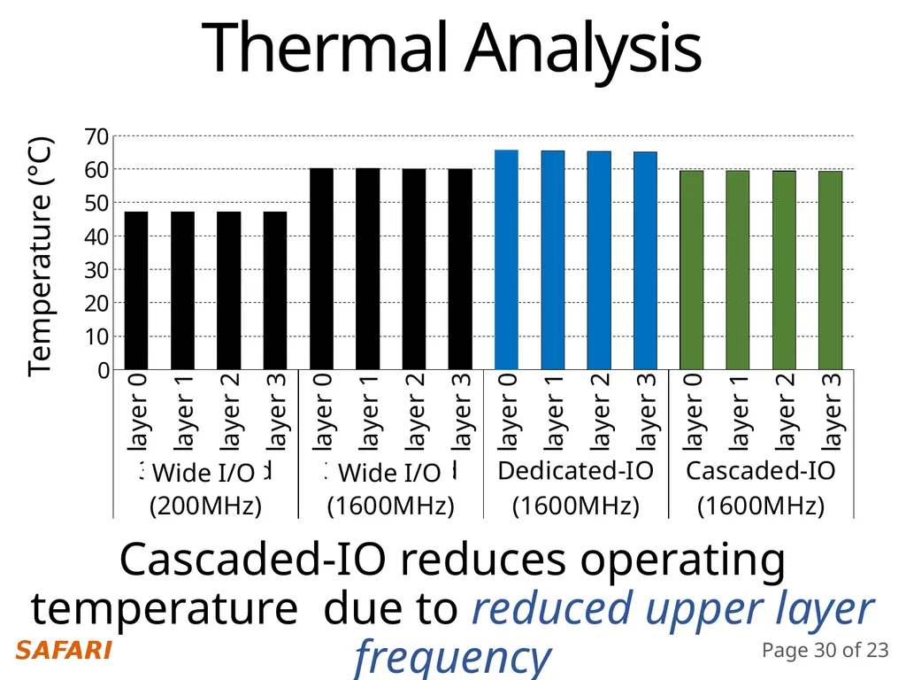
Thermal study
SMLA stays within DRAM operating range
Rank organization analysis
Scalability analysis for more DRAM layers<br>
22
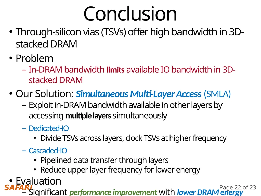
Conclusion Through-silicon vias (TSVs) offer high bandwidth in 3D-stacked DRAM
Problem
In-DRAM bandwidth limits available IO bandwidth in 3D-stacked DRAM
Our Solution: Simultaneous Multi-Layer Access (SMLA)
Exploit in-DRAM bandwidth available in other layers by accessing multiple layers simultaneously
Dedicated-IO
Divide TSVs across layers, clock TSVs at higher frequency
Cascaded-IO
Pipelined data transfer through layers
Reduce upper layer frequency for lower energy
Evaluation
Significant performance improvement with lower DRAM energy consumption (55%/18% for 16-core) at negligible DRAM area cost<br>
23
Donghyuk Lee, Saugata Ghose,�Gennady Pekhimenko, Samira Khan, Onur Mutlu
Carnegie Mellon University
HiPEAC 2016 We will release the SMLA source code by February. Simultaneous Multi-Layer Access�Improving 3D-Stacked Memory Bandwidth at Low Cost<br>
24
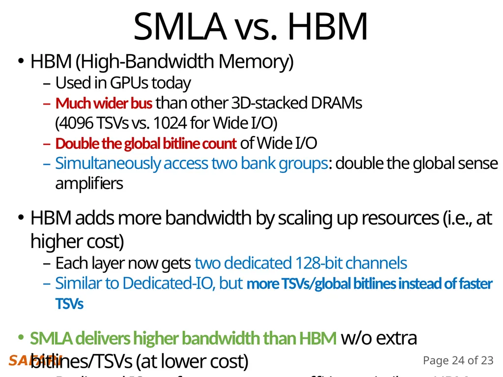
SMLA vs. HBM HBM (High-Bandwidth Memory)
Used in GPUs today
Much wider bus than other 3D-stacked DRAMs�(4096 TSVs vs. 1024 for Wide I/O)
Double the global bitline count of Wide I/O
Simultaneously access two bank groups: double the global sense amplifiers
HBM adds more bandwidth by scaling up resources (i.e., at higher cost)
Each layer now gets two dedicated 128-bit channels
Similar to Dedicated-IO, but more TSVs/global bitlines instead of faster TSVs
SMLA delivers higher bandwidth than HBM w/o extra bitlines/TSVs (at lower cost)
Dedicated-IO: performance, energy efficiency similar to HBM; cost is lower
Cascaded-IO: higher performance, energy efficiency; lower cost than HBM<br>
25
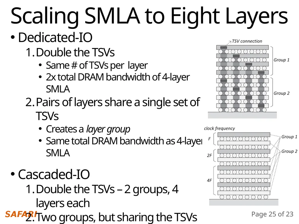
Scaling SMLA to Eight Layers Dedicated-IO
Double the TSVs
Same # of TSVs per layer
2x total DRAM bandwidth of 4-layer SMLA
Pairs of layers share a single set of TSVs
Creates a layer group
Same total DRAM bandwidth as 4-layer SMLA
Cascaded-IO
Double the TSVs – 2 groups, 4 layers each
Two groups, but sharing the TSVs
Groups necessary to stay within burst length, limit multi-layer traversal time
Same total DRAM bandwidth as 4-layer SMLA<br>
26
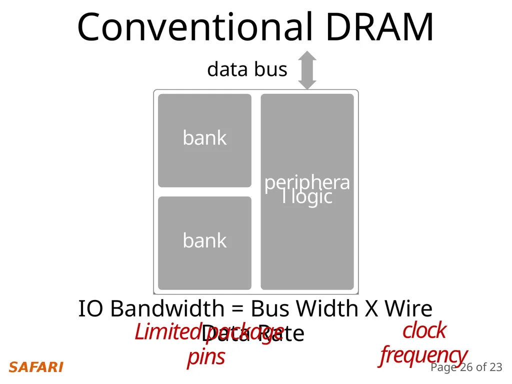
Conventional DRAM IO Bandwidth = Bus Width X Wire Data Rate Limited package pins clock frequency<br>
27
Cascaded-IO Operation data clock latch ctrl. data clock latch cell array &
peripheral logic cell array &
peripheral logic mux ctrl. mux counter en. counter en. 2F F data data 2B B<br>
28
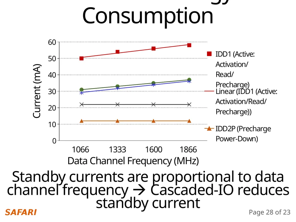
Estimated Energy Consumption 1066 1333 1600 1866 Data Channel Frequency (MHz) Current (mA) Standby currents are proportional to data channel frequency Cascaded-IO reduces standby current<br>
29
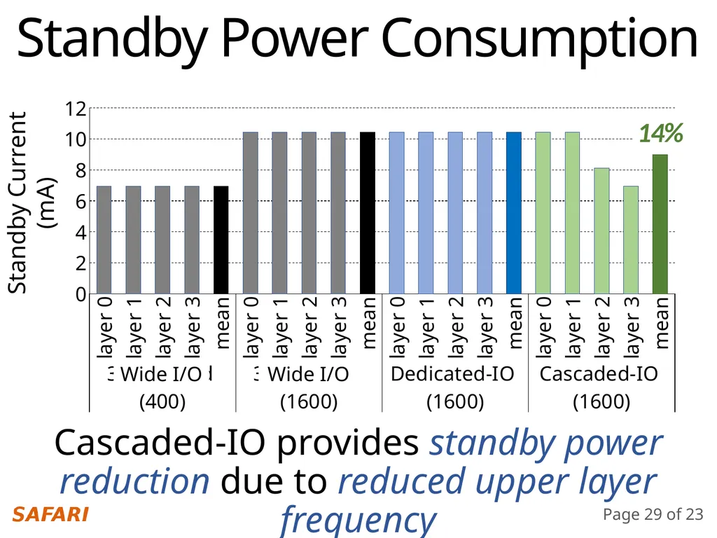
Standby Power Consumption Standby Current (mA) Cascaded-IO provides standby power reduction due to reduced upper layer frequency 14% Wide I/O Wide I/O<br>
30
Thermal Analysis Temperature (°C) Cascaded-IO reduces operating temperature due to reduced upper layer frequency Wide I/O Wide I/O<br>