
XIDyn High Flux, High Dynamic-range Hard X-ray




Description: XIDyn High Flux, High Dynamic-range Hard X-ray detector full-reticle ASIC for 4th generation synchrotrons Luke Mallett (RAL STFC) On behalf of the XIDyn Collaboration Introduction New generation of synchrotrons operate at significantly
Related Topics
Download Presentation
"XIDyn High Flux, High Dynamic-range Hard X-ray" is the property of its rightful owner. Permission is granted to download and print the materials on this website for personal, non-commercial use only, and to display it on your personal computer provided you do not modify the materials and that you retain all copyright notices contained in the materials. By downloading content from our website, you accept the terms of this agreement.
Presentation Transcript
slide1. XIDyn
High Flux, High Dynamic-range Hard X-ray detector full-reticle ASIC for 4th generation synchrotrons Luke Mallett (RAL STFC)
On behalf of the XIDyn Collaboration<br>
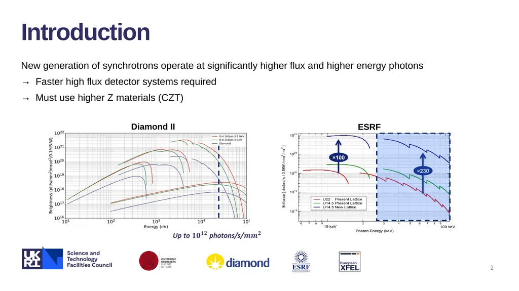
slide2. Introduction New generation of synchrotrons operate at significantly higher flux and higher energy photons
Faster high flux detector systems required
Must use higher Z materials (CZT) ESRF Diamond II 2<br>
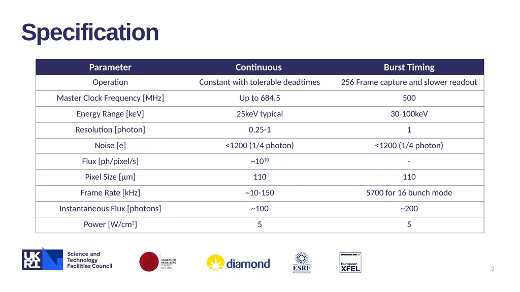
slide3. Specification 3<br>
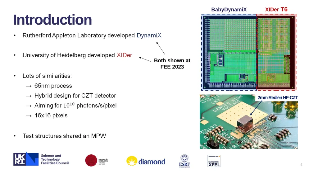
slide4. Introduction 4 2mm Redlen HF-CZT Both shown at
FEE 2023<br>
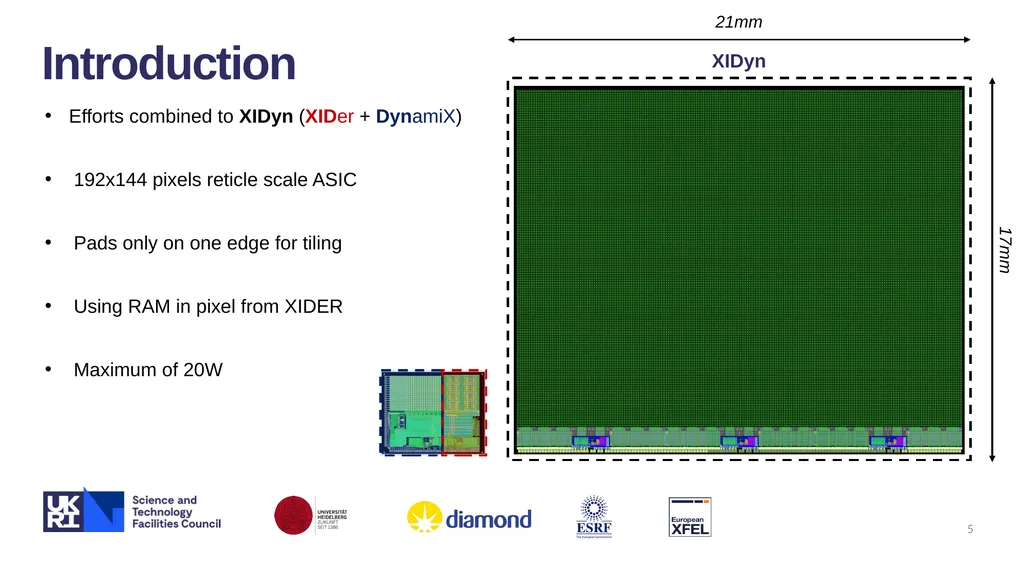
slide5. Introduction Efforts combined to XIDyn (XIDer + DynamiX)
192x144 pixels reticle scale ASIC
Pads only on one edge for tiling
Using RAM in pixel from XIDER
Maximum of 20W 21mm 17mm 5<br>
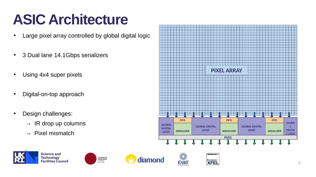
slide6. ASIC Architecture Large pixel array controlled by global digital logic
3 Dual lane 14.1Gbps serializers
Using 4x4 super pixels
Digital-on-top approach
Design challenges:
IR drop up columns
Pixel mismatch PADS PIXEL ARRAY 6<br>
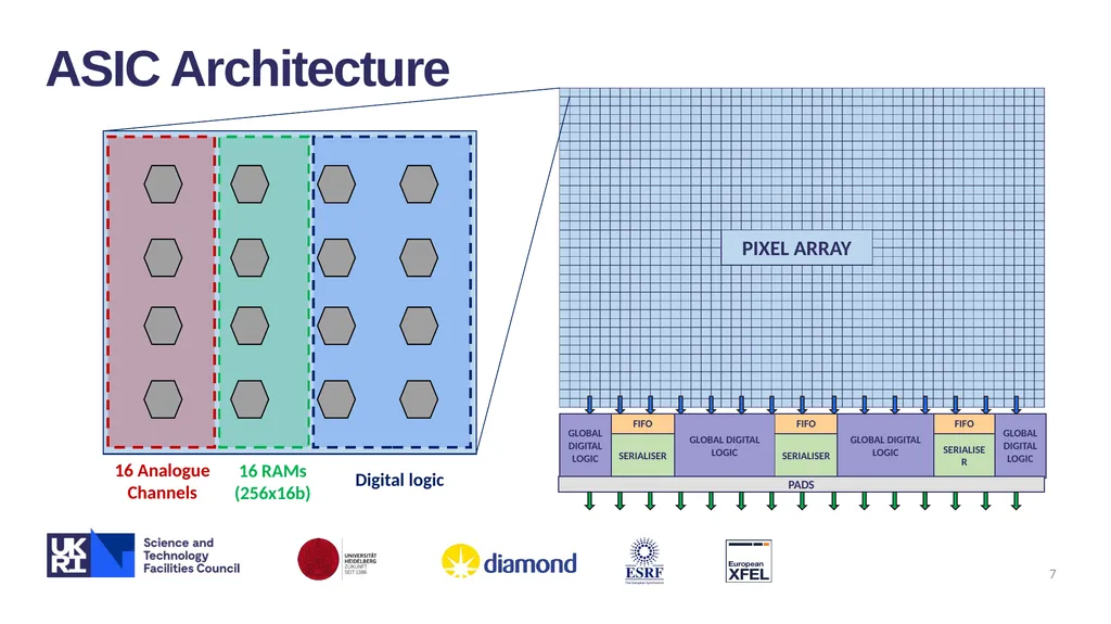
slide7. ASIC Architecture 16 Analogue Channels Digital logic 16 RAMs
(256x16b) PADS PIXEL ARRAY 7<br>
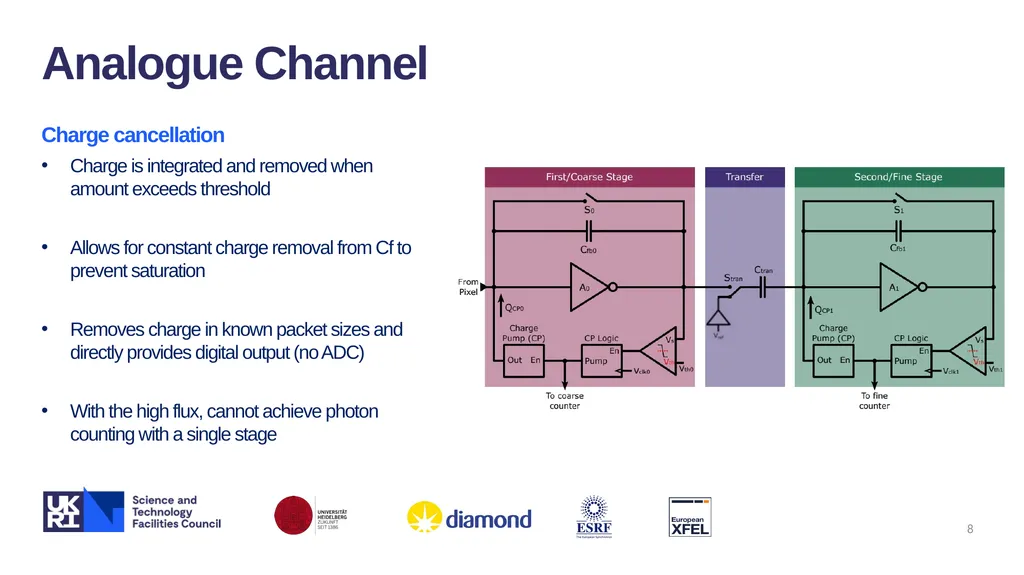
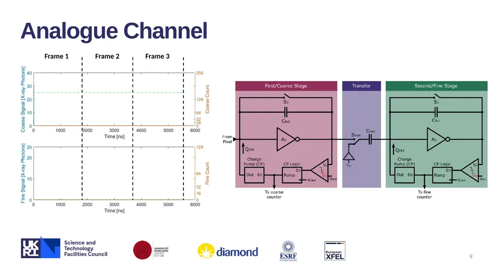
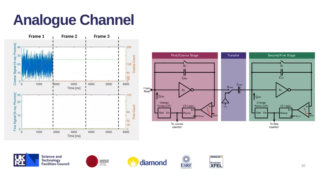
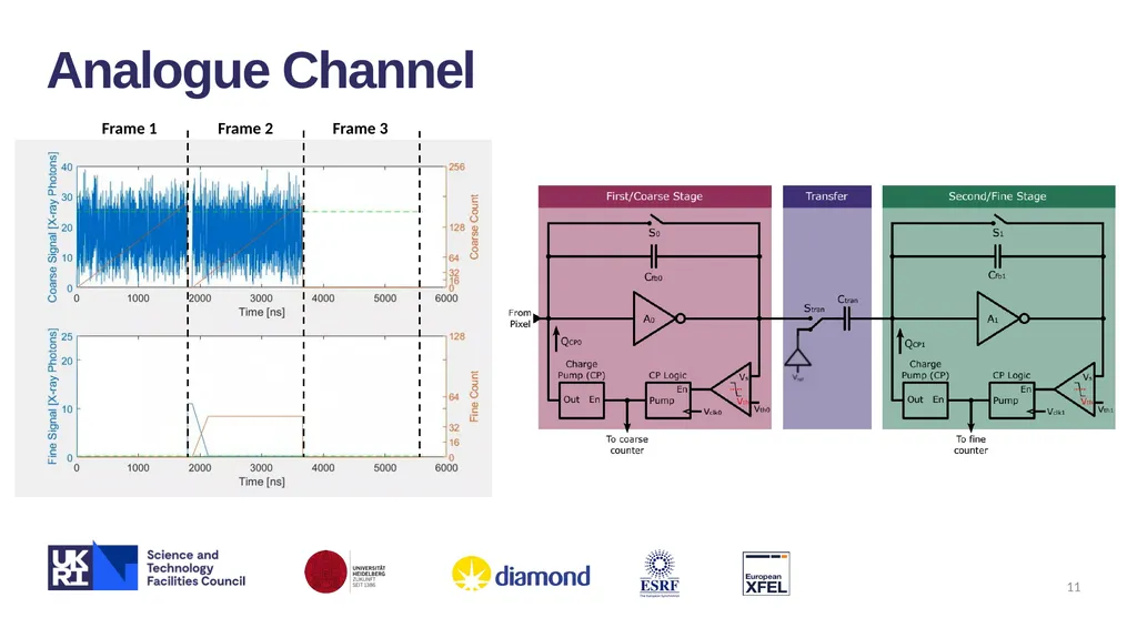
slide8. Analogue Channel Charge cancellation
Charge is integrated and removed when amount exceeds threshold
Allows for constant charge removal from Cf to prevent saturation
Removes charge in known packet sizes and directly provides digital output (no ADC)
With the high flux, cannot achieve photon counting with a single stage 8<br>
slide9. Analogue Channel Frame 1 Frame 2 Frame 3 9<br>
slide10. Analogue Channel Frame 1 Frame 2 Frame 3 10<br>
slide11. Analogue Channel Frame 1 Frame 2 Frame 3 11<br>
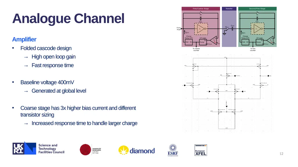
slide12. Analogue Channel Amplifier
Folded cascode design
High open loop gain
Fast response time
Baseline voltage 400mV
Generated at global level
Coarse stage has 3x higher bias current and different transistor sizing
Increased response time to handle larger charge Coarse stage has 3x higher bias current WHY 12<br>
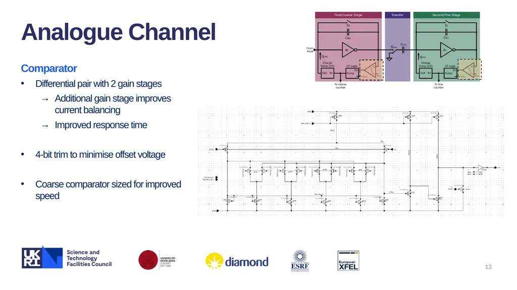
slide13. Analogue Channel Comparator
Differential pair with 2 gain stages
Additional gain stage improves current balancing
Improved response time
4-bit trim to minimise offset voltage
Coarse comparator sized for improved speed 13<br>
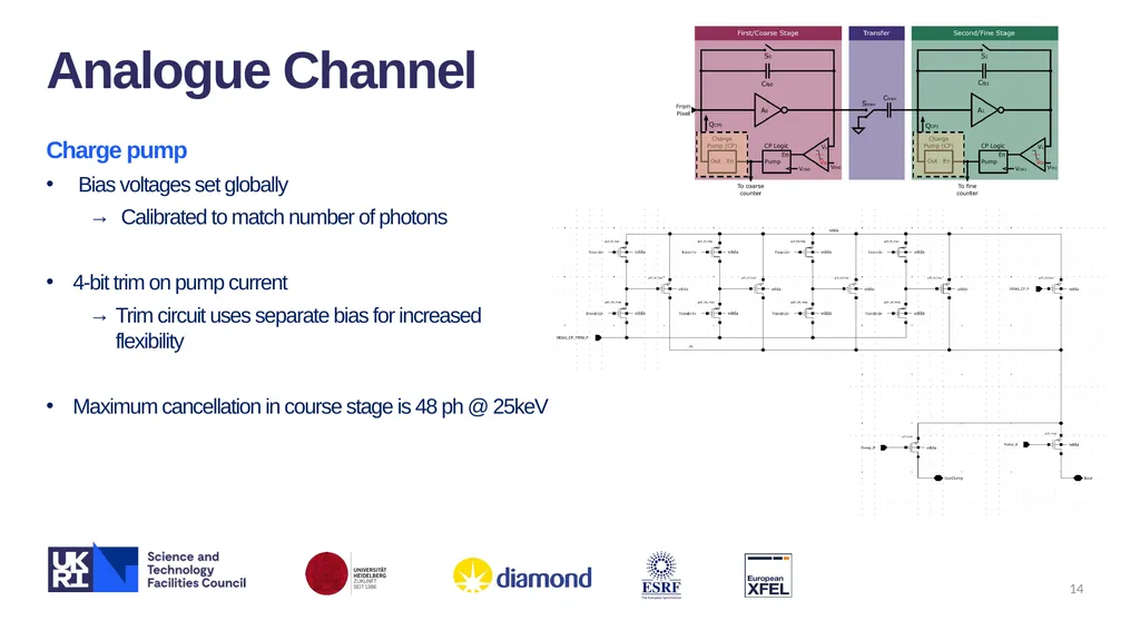
slide14. Analogue Channel Pump time in multiples of Master Clock period
Current either pumped into channel or dumped to ground 14 Charge pump
Bias voltages set globally
Calibrated to match number of photons
4-bit trim on pump current
Trim circuit uses separate bias for increased flexibility
Maximum cancellation in course stage is 48 ph @ 25keV<br>
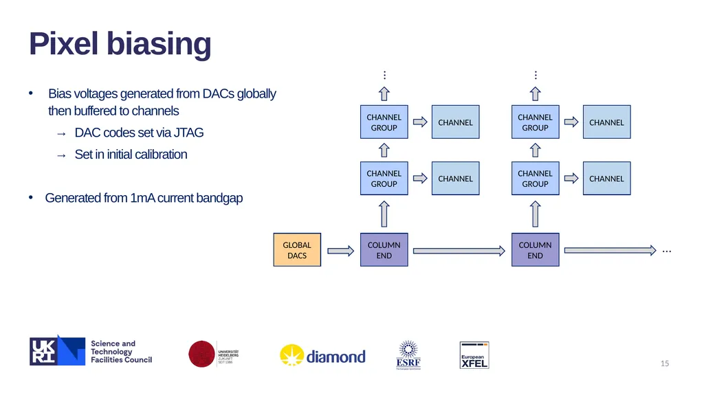
slide15. Pixel biasing Bias voltages generated from DACs globally then buffered to channels
DAC codes set via JTAG
Set in initial calibration
Generated from 1mA current bandgap GLOBAL DACS COLUMN END CHANNEL GROUP CHANNEL CHANNEL GROUP CHANNEL … COLUMN END CHANNEL GROUP CHANNEL CHANNEL GROUP CHANNEL … … 15<br>
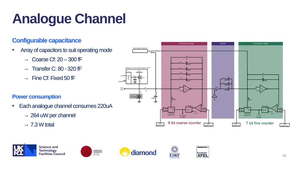
slide16. Analogue Channel Configurable capacitance
Array of capacitors to suit operating mode
Coarse Cf: 20 – 300 fF
Transfer C: 80 - 320 fF
Fine Cf: Fixed 50 fF
Power consumption
Each analogue channel consumes 220uA
264 uW per channel
7.3 W total 16<br>
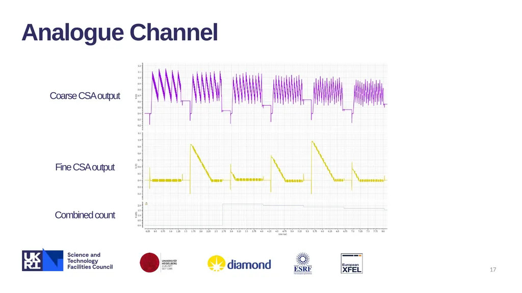
slide17. Analogue Channel Fine CSA output Combined count 17 Coarse CSA output<br>
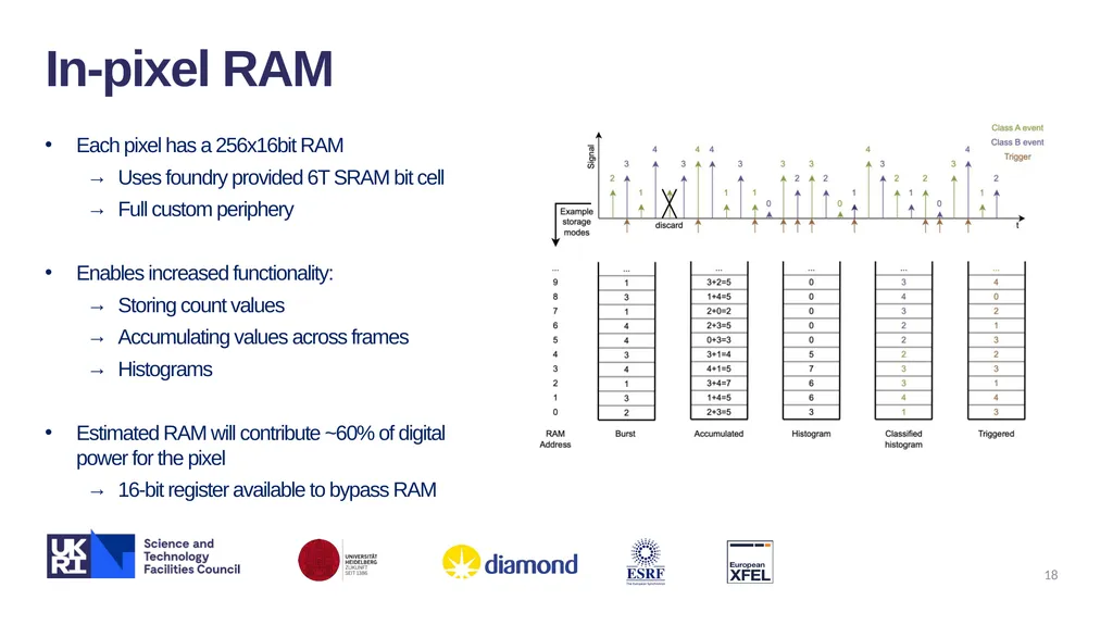
slide18. In-pixel RAM Each pixel has a 256x16bit RAM
Uses foundry provided 6T SRAM bit cell
Full custom periphery
Enables increased functionality:
Storing count values
Accumulating values across frames
Histograms
Estimated RAM will contribute ~60% of digital power for the pixel
16-bit register available to bypass RAM 18<br>
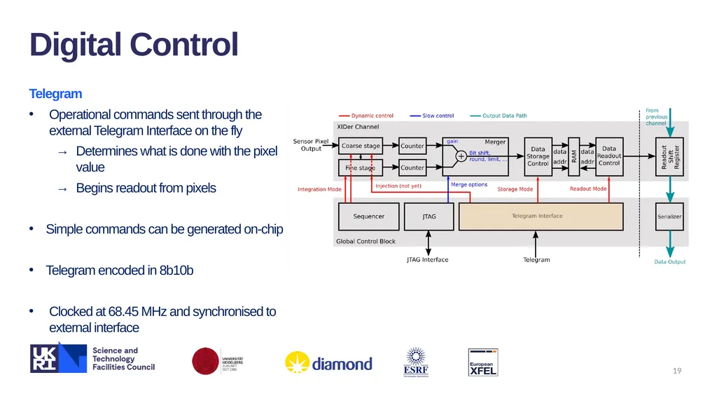
slide19. Digital Control Telegram
Operational commands sent through the external Telegram Interface on the fly
Determines what is done with the pixel value
Begins readout from pixels
Simple commands can be generated on-chip
Telegram encoded in 8b10b
Clocked at 68.45 MHz and synchronised to external interface 19<br>
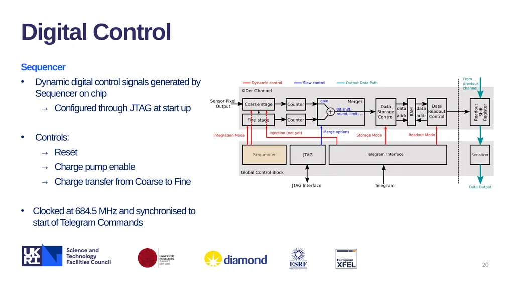
slide20. Digital Control Sequencer
Dynamic digital control signals generated by Sequencer on chip
Configured through JTAG at start up
Controls:
Reset
Charge pump enable
Charge transfer from Coarse to Fine
Clocked at 684.5 MHz and synchronised to start of Telegram Commands 20<br>
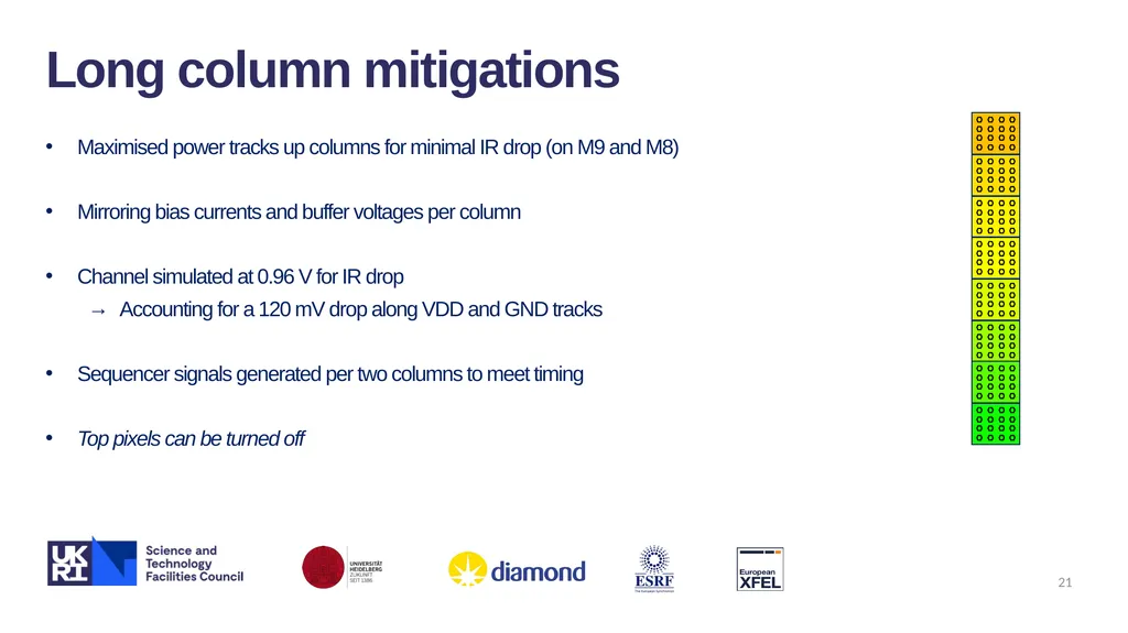
slide21. Long column mitigations Maximised power tracks up columns for minimal IR drop (on M9 and M8)
Mirroring bias currents and buffer voltages per column
Channel simulated at 0.96 V for IR drop
Accounting for a 120 mV drop along VDD and GND tracks
Sequencer signals generated per two columns to meet timing
Top pixels can be turned off 21<br>
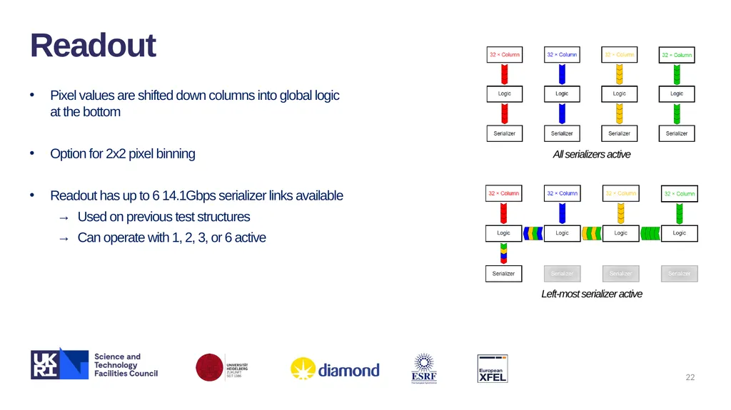
slide22. Readout Pixel values are shifted down columns into global logic at the bottom
Option for 2x2 pixel binning
Readout has up to 6 14.1Gbps serializer links available
Used on previous test structures
Can operate with 1, 2, 3, or 6 active 22<br>
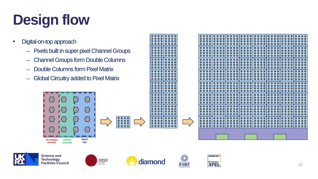
slide23. Design flow Digital-on-top approach
Pixels built in super pixel Channel Groups
Channel Groups form Double Columns
Double Columns form Pixel Matrix
Global Circuitry added to Pixel Matrix 23<br>
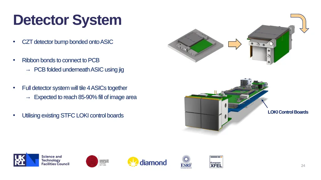
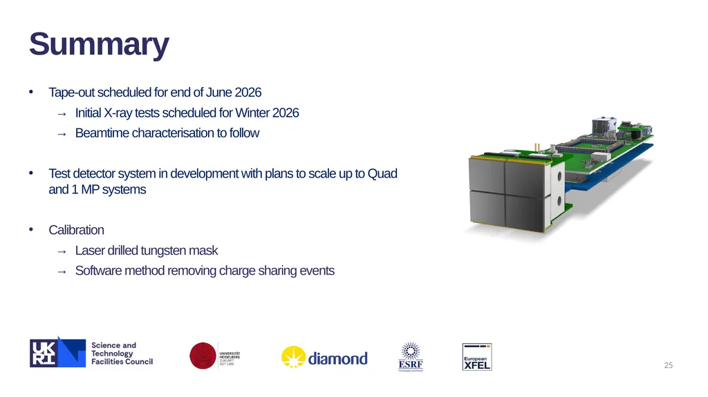
slide24. Detector System CZT detector bump bonded onto ASIC
Ribbon bonds to connect to PCB
PCB folded underneath ASIC using jig
Full detector system will tile 4 ASICs together
Expected to reach 85-90% fill of image area
Utilising existing STFC LOKI control boards 24 LOKI Control Boards<br>
slide25. Summary Tape-out scheduled for end of June 2026
Initial X-ray tests scheduled for Winter 2026
Beamtime characterisation to follow
Test detector system in development with plans to scale up to Quad and 1 MP systems
Calibration
Laser drilled tungsten mask
Software method removing charge sharing events 25<br>
slide26. 26<br>
slide27. @STFC_matters Science and Technology Facilities Council Science and Technology Facilities Council 27<br>
slide28. Backup 28<br>
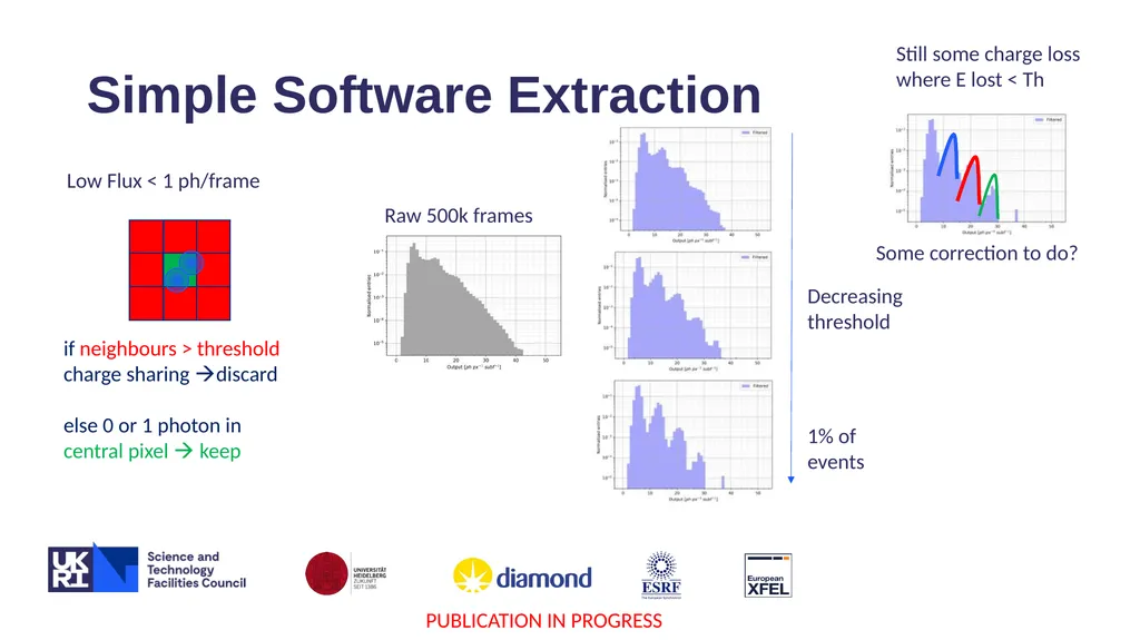
slide29. Simple Software Extraction Low Flux < 1 ph/frame if neighbours > threshold charge sharing discard
else 0 or 1 photon in
central pixel keep Raw 500k frames Decreasing threshold 1% of events PUBLICATION IN PROGRESS<br>
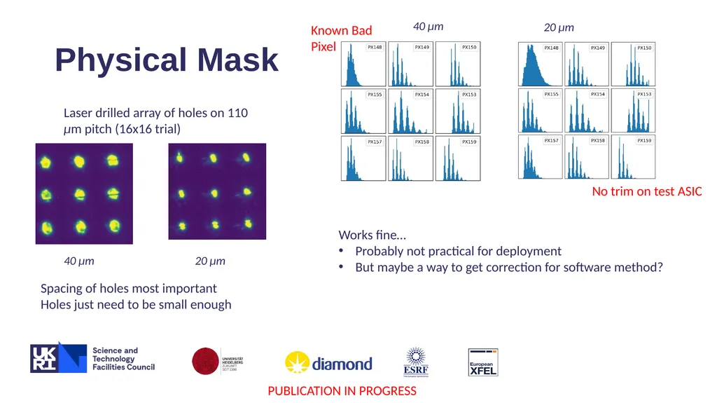
slide30. Physical Mask 20 µm 40 µm Laser drilled array of holes on 110 µm pitch (16x16 trial) Known Bad Pixel No trim on test ASIC 40 µm 20 µm Spacing of holes most important
Holes just need to be small enough Works fine…
Probably not practical for deployment
But maybe a way to get correction for software method? PUBLICATION IN PROGRESS<br>
High Flux, High Dynamic-range Hard X-ray detector full-reticle ASIC for 4th generation synchrotrons Luke Mallett (RAL STFC)
On behalf of the XIDyn Collaboration<br>
slide2. Introduction New generation of synchrotrons operate at significantly higher flux and higher energy photons
Faster high flux detector systems required
Must use higher Z materials (CZT) ESRF Diamond II 2<br>
slide3. Specification 3<br>
slide4. Introduction 4 2mm Redlen HF-CZT Both shown at
FEE 2023<br>
slide5. Introduction Efforts combined to XIDyn (XIDer + DynamiX)
192x144 pixels reticle scale ASIC
Pads only on one edge for tiling
Using RAM in pixel from XIDER
Maximum of 20W 21mm 17mm 5<br>
slide6. ASIC Architecture Large pixel array controlled by global digital logic
3 Dual lane 14.1Gbps serializers
Using 4x4 super pixels
Digital-on-top approach
Design challenges:
IR drop up columns
Pixel mismatch PADS PIXEL ARRAY 6<br>
slide7. ASIC Architecture 16 Analogue Channels Digital logic 16 RAMs
(256x16b) PADS PIXEL ARRAY 7<br>
slide8. Analogue Channel Charge cancellation
Charge is integrated and removed when amount exceeds threshold
Allows for constant charge removal from Cf to prevent saturation
Removes charge in known packet sizes and directly provides digital output (no ADC)
With the high flux, cannot achieve photon counting with a single stage 8<br>
slide9. Analogue Channel Frame 1 Frame 2 Frame 3 9<br>
slide10. Analogue Channel Frame 1 Frame 2 Frame 3 10<br>
slide11. Analogue Channel Frame 1 Frame 2 Frame 3 11<br>
slide12. Analogue Channel Amplifier
Folded cascode design
High open loop gain
Fast response time
Baseline voltage 400mV
Generated at global level
Coarse stage has 3x higher bias current and different transistor sizing
Increased response time to handle larger charge Coarse stage has 3x higher bias current WHY 12<br>
slide13. Analogue Channel Comparator
Differential pair with 2 gain stages
Additional gain stage improves current balancing
Improved response time
4-bit trim to minimise offset voltage
Coarse comparator sized for improved speed 13<br>
slide14. Analogue Channel Pump time in multiples of Master Clock period
Current either pumped into channel or dumped to ground 14 Charge pump
Bias voltages set globally
Calibrated to match number of photons
4-bit trim on pump current
Trim circuit uses separate bias for increased flexibility
Maximum cancellation in course stage is 48 ph @ 25keV<br>
slide15. Pixel biasing Bias voltages generated from DACs globally then buffered to channels
DAC codes set via JTAG
Set in initial calibration
Generated from 1mA current bandgap GLOBAL DACS COLUMN END CHANNEL GROUP CHANNEL CHANNEL GROUP CHANNEL … COLUMN END CHANNEL GROUP CHANNEL CHANNEL GROUP CHANNEL … … 15<br>
slide16. Analogue Channel Configurable capacitance
Array of capacitors to suit operating mode
Coarse Cf: 20 – 300 fF
Transfer C: 80 - 320 fF
Fine Cf: Fixed 50 fF
Power consumption
Each analogue channel consumes 220uA
264 uW per channel
7.3 W total 16<br>
slide17. Analogue Channel Fine CSA output Combined count 17 Coarse CSA output<br>
slide18. In-pixel RAM Each pixel has a 256x16bit RAM
Uses foundry provided 6T SRAM bit cell
Full custom periphery
Enables increased functionality:
Storing count values
Accumulating values across frames
Histograms
Estimated RAM will contribute ~60% of digital power for the pixel
16-bit register available to bypass RAM 18<br>
slide19. Digital Control Telegram
Operational commands sent through the external Telegram Interface on the fly
Determines what is done with the pixel value
Begins readout from pixels
Simple commands can be generated on-chip
Telegram encoded in 8b10b
Clocked at 68.45 MHz and synchronised to external interface 19<br>
slide20. Digital Control Sequencer
Dynamic digital control signals generated by Sequencer on chip
Configured through JTAG at start up
Controls:
Reset
Charge pump enable
Charge transfer from Coarse to Fine
Clocked at 684.5 MHz and synchronised to start of Telegram Commands 20<br>
slide21. Long column mitigations Maximised power tracks up columns for minimal IR drop (on M9 and M8)
Mirroring bias currents and buffer voltages per column
Channel simulated at 0.96 V for IR drop
Accounting for a 120 mV drop along VDD and GND tracks
Sequencer signals generated per two columns to meet timing
Top pixels can be turned off 21<br>
slide22. Readout Pixel values are shifted down columns into global logic at the bottom
Option for 2x2 pixel binning
Readout has up to 6 14.1Gbps serializer links available
Used on previous test structures
Can operate with 1, 2, 3, or 6 active 22<br>
slide23. Design flow Digital-on-top approach
Pixels built in super pixel Channel Groups
Channel Groups form Double Columns
Double Columns form Pixel Matrix
Global Circuitry added to Pixel Matrix 23<br>
slide24. Detector System CZT detector bump bonded onto ASIC
Ribbon bonds to connect to PCB
PCB folded underneath ASIC using jig
Full detector system will tile 4 ASICs together
Expected to reach 85-90% fill of image area
Utilising existing STFC LOKI control boards 24 LOKI Control Boards<br>
slide25. Summary Tape-out scheduled for end of June 2026
Initial X-ray tests scheduled for Winter 2026
Beamtime characterisation to follow
Test detector system in development with plans to scale up to Quad and 1 MP systems
Calibration
Laser drilled tungsten mask
Software method removing charge sharing events 25<br>
slide26. 26<br>
slide27. @STFC_matters Science and Technology Facilities Council Science and Technology Facilities Council 27<br>
slide28. Backup 28<br>
slide29. Simple Software Extraction Low Flux < 1 ph/frame if neighbours > threshold charge sharing discard
else 0 or 1 photon in
central pixel keep Raw 500k frames Decreasing threshold 1% of events PUBLICATION IN PROGRESS<br>
slide30. Physical Mask 20 µm 40 µm Laser drilled array of holes on 110 µm pitch (16x16 trial) Known Bad Pixel No trim on test ASIC 40 µm 20 µm Spacing of holes most important
Holes just need to be small enough Works fine…
Probably not practical for deployment
But maybe a way to get correction for software method? PUBLICATION IN PROGRESS<br>