/
Lecture  10 Direct and Indirect Band Lecture  10 Direct and Indirect Band

Lecture 10 Direct and Indirect Band - PowerPoint Presentation

zoe
zoe . @zoe
Follow
65 views
Uploaded On 2023-11-11

Lecture 10 Direct and Indirect Band - PPT Presentation

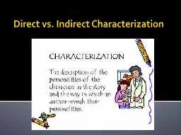
Gap 1 Recap Most energy bands are close to parabolic at their minima for conduction band or maxima for valence band In the reciprocal space at reciprocal lattice points electron undergoes diffraction by the lattice causing a discontinuity in the E k diagram ID: 1031197

energy band momentum gap band energy gap momentum semiconductor photon direct electron conduction indirect valence crystal difference ibg dbg

Share:

Link:

Embed:

Download Presentation from below link

Download Presentation The PPT/PDF document "Lecture 10 Direct and Indirect Band" is the property of its rightful owner. Permission is granted to download and print the materials on this web site for personal, non-commercial use only, and to display it on your personal computer provided you do not modify the materials and that you retain all copyright notices contained in the materials. By downloading content from our website, you accept the terms of this agreement.


Presentation Transcript

1. Lecture 10Direct and Indirect Band Gap1

2. RecapMost energy bands are close to parabolic at their minima (for conduction band) or maxima for valence band. In the reciprocal space at reciprocal lattice points electron undergoes diffraction by the lattice, causing a discontinuity in the E k diagram.These discontinuities at these points are basically the gaps states. As energy increases , the gaps become larger and larger. 2

3. Dynamics of Charge CarriersThe force on a charge carrier in a crystal is F = m*a, or the product of “effective mass” and acceleration. This makes the kinetic energy of a charge carrier in a crystalWhere p is the momentum of the charge carrier and m* is the effective mass. Furthermore, during electron excitation, a photon is absorbed by an electron, and therefore the energy difference between the electron’s final and initial energy states is the energy of the photon. Thus we have thatwhere Ee is the original energy of the crystal, Ea is the final state of the crystal after the photon is absorbed, h is Planck’s constant, and f is the corresponding frequency of the photon.3

4. Dynamics of Charge CarriersThe matching equations for the energies of an electron in the conduction band and hole in the valence band are as follows:where Ec is the energy level of the minimum edge of the conduction band, Ev is the energy at the edge of the valence band, and mn* and mp* are the effective masses of electrons and holes respectively (which are actually different from each other). 4

5. Dynamics of Charge CarriersThese equations mean that the electron’s energy due to its momentum is the difference between its “relaxed” state of the crystal before photon absorption and the conduction band energy level, And the hole’s energy is the difference between its energy state in the valence band and the energy of the crystal after photon absorption. These equations are just a result of conservation of energy and momentum; the photon absorption must result in an energy change in both the electron and hole in such a way that the momentum of each is increased with kinetic energy. 5

6. Dynamics of Charge CarriersAbsorption Coefficient for Direct SemiconductorsAdding the two previous equations together produces a very useful result for explaining absorption in a certain class of semiconductors. If we do this, we getwhere Eg is the energy required to cross the band gap and hf is the energy of the absorbed photon. It turns out this equation holds true for a type of semiconductor called a direct semiconductor, because the absorption conditions are purely based on the band gap of the material and the photon energy. This is because the curves relating energy to crystal momentum are aligned, and therefore the crystal momentum increases directly as a result of increased photon energy.6

7. Figure1 The valence band and conduction band curves in a graph of energy vs. crystal momentum are aligned if the semiconductor has a direct band gap7

8. Direct Band GapThe band gap represents the minimum energy difference between the top of the valence band and the bottom of the conduction band.However, the top of the valence band and the bottom of the conduction band are not generally at the same value of the electron momentum. In a direct band gap semiconductor, the top of the valence band and the bottom of the conduction band occur at the same value of momentum8

9. Generalizing the Absorption CoefficientWe can think of the curves of the two bands as being “misaligned”, with minimums/maximums being separated by some distance on the crystal momentum axis. Therefore, the minimum of the conduction band would be at some finite value of crystal momentum such that:where p0 and p0' are the respective shifts in the crystal momentum for the conduction and valence bands We can see from these equations that if p0 = p0', the semiconductor has a direct band gap, because an increase in photon energy directly correlates to an increase in crystal momentum. If p0 ≠ p0', then the band gap is called indirect. 9

10. Indirect band gap semiconductorIn an indirect band gap semiconductor, the maximum energy of the valence band occurs at a different value of momentum to the minimum in the conduction band energy:10

11. Difference between Direct and Indirect Band GapA photon can provide the energy to produce an electron-hole pair. Each photon of energy E has momentum p = E / c, where c is the velocity of light. An optical photon has an energy of the order of 10–19 J, and, since c = 3 × 108 ms–1, a typical photon has a very small amount of momentum. A photon of energy Eg, where Eg is the band gap energy, can produce an electron-hole pair in a direct band gap semiconductor quite easily, because the electron does not need to be given very much momentum. However, an electron must also undergo a significant change in its momentum for a photon of energy Eg to produce an electron-hole pair in an indirect band gap semiconductor. This is possible, but it requires such an electron to interact not only with the photon to gain energy, but also with a lattice vibration called a phonon in order to either gain or lose momentum. 11

12. Difference between Direct and Indirect Band GapThe indirect process proceeds at a much slower rate, as it requires three entities to intersect in order to proceed: an electron, a photon and a phonon. This is analogous to chemical reactions, where, in a particular reaction step, a reaction between two molecules will proceed at a much greater rate than a process which involves three molecules. The same principle applies to recombination of electrons and holes to produce photons. The recombination process is much more efficient for a direct band gap semiconductor than for an indirect band gap semiconductor, where the process must be mediated by a phonon. 12

13. Difference between Direct and Indirect Band GapAs a result of such considerations, gallium arsenide and other direct band gap semiconductors are used to make optical devices such as LEDs and semiconductor lasers, whereas silicon, which is an indirect band gap semiconductor, is not13

14. Direct band-gap (DBG) semiconductorIndirect band-gap (IBG) semiconductorA direct band-gap (DBG) semiconductor is one in which the maximum energy level of the valence band aligns with the minimum energy level of the conduction band with respect to momentum. In a DBG semiconductor, a direct recombination takes place with the release of the energy equal to the energy difference between the recombining particles.   The probability of a radiative recombination is high.An Indirect band-gap (IBG) semiconductor is one in which the maximum energy level of the valence band and the minimum energy level of the conduction band are misaligned with respect to momentum. In case of a IBG semiconductor, due to a relative difference in the momentum, first, the momentum is conserved by release of energy and only after the both the momenta align themselves, a recombination occurs accompanied with the release of energy.  The probability of a radiative recombination is comparatively low.14

15. Direct band-gap (DBG) semiconductorIndirect band-gap (IBG) semiconductorThe efficiency factor of a DBG semiconductor is higher. Thus, DBG semiconductors are always preferred over IBG for making optical sources.A photon of energy Eg, where Eg is the band gap energy, can produce an electron-hole pair in a direct band gap semiconductor quite easily, because the electron does not need to be given very much momentum. The most thoroughly investigated and studied DBG semiconductor material is Gallium Arsenide (GaAs).  DBG semiconductors are always preferred over IBG for making optical sources.The efficiency factor of a IBG semiconductor is lower.   The indirect process proceeds at a much slower rate, as it requires three entities to intersect in order to proceed: an electron, a photon and a phonon.  The two well-known intrinsic semiconductors, Silicon and Germanium are both IBG semiconductors.  The IBG semiconductors cannot be used to manufacture optical sources. 15

16. SummaryDifference between Direct and Indirect Semiconductor was discussed.In a direct band gap semiconductor, the top of the valence band and the bottom of the conduction band occur at the same value of momentumIn an indirect band gap semiconductor, the maximum energy of the valence band occurs at a different value of momentum to the minimum in the conduction band energy:16