PPT-Chemical Nanoparticle Deposition of Oxide Nanostructured Thin Films
Author : aaron | Published Date : 2018-11-08
6 Conclusions 2 Experimental Setup 1 Abstract We have developed a novel approach to deposit oxide nanostructured thin films via a simple solution chemistry This
Presentation Embed Code
Download Presentation
Download Presentation The PPT/PDF document "Chemical Nanoparticle Deposition of Oxid..." is the property of its rightful owner. Permission is granted to download and print the materials on this website for personal, non-commercial use only, and to display it on your personal computer provided you do not modify the materials and that you retain all copyright notices contained in the materials. By downloading content from our website, you accept the terms of this agreement.
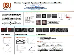
Chemical Nanoparticle Deposition of Oxide Nanostructured Thin Films: Transcript
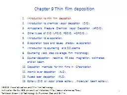
6 Conclusions 2 Experimental Setup 1 Abstract We have developed a novel approach to deposit oxide nanostructured thin films via a simple solution chemistry This approach uses a continuousflow microreactor to continuously generate a flux of nanoparticles which then impinge on a heated substrate surface The thin film formation follows a simple particle sticking mechanism For example highly transparent nanocrystalline ZnO thin films and exhibit a larger optical bandgap at 435 eV were deposited using this technique Functional ZnO MISFETs were successfully fabricated using this technique after a post air annealing process In addition to ZnO we have also deposited Fe. Oladeji Guangyu Chai Lee Chow a Department of Physics University of Central Florida Orlando FL 32816 USA SOLMAX TECHNOLOGIES 1209 West Gore St Orlando FL 32805 USA Apollo Technologies Inc 205 Waymont Court Suite 111 Lake Mary FL 32746 USA Received (PVD and CVD). 1. Plan of presentation. Deposition methods. . CVD(. . Chemical . Vapor . Deposition) . . PVD ( Physical . Vapor . Deposition. ). Principles, processes on . the surface . . 2. International. Contact us at: contact.omics@omicsonline.org. OMICS . International through . its Open Access Initiative is committed to make genuine and reliable contributions to the scientific . community. OMICS International . for the . Transmission . of . Visible . and . Infrared Radiation. Carlos M. . Bledt. . a. and . James A. Harrington . a. a. Dept. of Material Science & Engineering . Rutgers, the State University of New Jersey. Phenomena. : . Block copolymer (BCPs) in thin films with . long range lateral order. ,. self-assembly. and so on….. Block Copolymers (BCPs) in thin films. Physics. : . We consider aspects of. segmental interactions. OMICS . International through . its Open Access Initiative is committed to make genuine and reliable contributions to the scientific . community. OMICS International . journals have over . 3 million. Carlos M. . Bledt. *. a. , Daniel V. Kopp . a. , and James A. Harrington . a. a. Dept. of Material Science & Engineering . Rutgers, the State University of New Jersey. Jason M. . Kriesel. . b. b. for . Sensor . and . Laser Power Delivery Applications. Theory, Design, and Fabrication. Carlos M. . Bledt. . a. , James A. Harrington . a. , and Jason M. . Kriesel. . b. a. Dept. of Material Science & Engineering . Introduction to thin film deposition.. Introduction to chemical vapor deposition (CVD).. Atmospheric Pressure Chemical Vapor Deposition (APCVD).. Other types of CVD (LPCVD, PECVD, HDPCVD…).. Introduction to evaporation.. a. LIGO. Carmen S. Menoni. Electrical & Computer Engineering. Colorado State University. Collaborators: . Le Yang (Grad. Student), Mariana Fazio (post-doctoral student), Colorado State University. in ASTeC. Oleg Malyshev and Reza Valizadeh. 1. The aim of TF SRF programme. SRF programme at ASTeC started six years ago from no infrastructure and it aims from beginning was to stablish know how for depositing SRF thin film in RF (. Somesh Kr Malhotra. Assistant Professor. ECE . Department,UIET. Introduction. Thin film circuits consist of conductor layers, resistor layers and dielectric layers, similarly to thick film circuits. However, the thin film thicknesses are normally 1 µm or less, an order of magnitude less than for thick film. . Prof. . Dr. . Wisam. J. Aziz . Solid state physics. Lecture (10). Chemical Deposition Techniques. Chemical deposition is one fabrication technique, whereby the material to be coated are allowed to react to different chemicals allowing specific reactions to take place in a way that the coating forms . PHYS 1600. September 27, 2021. PROBLEM. : How do we make useful devices – especially electronic circuits – from scratch?. Solder them together from components? . Sep. 27, 2021. 2. Need millions of diode/transistor circuits to achieve the computing speeds, and the densities of memory required!.
Download Document
Here is the link to download the presentation.
"Chemical Nanoparticle Deposition of Oxide Nanostructured Thin Films"The content belongs to its owner. You may download and print it for personal use, without modification, and keep all copyright notices. By downloading, you agree to these terms.
Related Documents