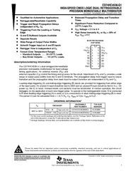
/
CDHCQ HIGHSPEED CMOS LOGIC DUAL RETRIGGERABLE PRECISION MONOSTABLE MULTIVIBRATOR SCLSA CDHCQ HIGHSPEED CMOS LOGIC DUAL RETRIGGERABLE PRECISION MONOSTABLE MULTIVIBRATOR SCLSA

CDHCQ HIGHSPEED CMOS LOGIC DUAL RETRIGGERABLE PRECISION MONOSTABLE MULTIVIBRATOR SCLSA - PDF document

alida-meadow
alida-meadow . @alida-meadow
Follow
495 views
Uploaded On 2014-12-18

CDHCQ HIGHSPEED CMOS LOGIC DUAL RETRIGGERABLE PRECISION MONOSTABLE MULTIVIBRATOR SCLSA - PPT Presentation

10 LSTTL Loads 8722 Bus Driver Outputs 15 LSTTL Loads Balanced Propagation Delay and Transition Times Significant Power Reduction Compared to LSTTL Logic ICs CC Voltage 2 V to 6 V High Noise Immunity N IL or N IH 30 of CC V CC 5 V descriptionor ID: 25928

LSTTL Loads 8722

Share:

Link:

Embed:

Download Presentation from below link

Download Pdf The PPT/PDF document "CDHCQ HIGHSPEED CMOS LOGIC DUAL RETRIGGE..." is the property of its rightful owner. Permission is granted to download and print the materials on this web site for personal, non-commercial use only, and to display it on your personal computer provided you do not modify the materials and that you retain all copyright notices contained in the materials. By downloading content from our website, you accept the terms of this agreement.


Presentation Transcript

PRECISION MONOSTABLE MULTIVIBRATOR SCLS595A  POST OFFICE BOX 655303 DALLAS, TEXAS 75265Trigger and Reset Propagation DelaysTriggering From the Leading or Trailing Buffered Outputs AvailableWide Range of Output Pulse Widths Retrigger Time Is Independent of CFanout (Over Temperature Range)... 10 ... 15 Balanced Propagation Delay and TransitionTimes Voltage = 2 V to 6 Vdescription/ordering informationprecision monostable multivibrator for fixed-voltagetiming applications. An external resistor (Rexternal range of output pulse widths from the Q and Q terminals. The propagation delay from trigger input-to-output of the input pulse. An unused A input should be tied to GND and an unused B . Onpower up, the IC is reset. Unused resets and sections must be terminated. In normal operation, the circuiton the application of each new trigger pulse. To operate in the nontriggerable mode, Q to B when leading-edge triggering (A) is used, or Q is connected to A when trailing-edge triggering (B is 0 pF.ORDERING INFORMATION PACKAGE ORDERABLE TOP-SIDE Cto125 Tape and reel HC4538M 40°C Tape and reel HC4538M end of this document, or see the TI web site at http://www.ti.com.are available at http://www.ti.com/packaging.Copyright 2008, Texas Instruments IncorporatedPRODUCTION DATA information is current as of publication date.Products conform to specifications per the terms of Texas Instrumentsstandard warranty. Production processing does not necessarily include Please be aware that an important notice concerning availability, standard warranty, and use in critical applications ofTexasInstruments semiconductor products and disclaimers thereto appears at the end of this data sheet. M OR PW PACKAGE(TOP VIEW) 1236781615141291CX1RXCX1R 1A1B 1Q1Q GNDVX2RXCX2R 2A2B 2Q PRECISION MONOSTABLE MULTIVIBRATORSCLS595A  POST OFFICE BOX 655303 DALLAS, TEXAS 75265FUNCTION TABLE OUTPUTS R A B Q Q L X X L H X HXL X XLL H L H  H NOTE:H = High voltage level = Transition from low to high level = Transition from high to low level logic diagram (positive logic) 5(11) R1R2 FF Q PRECISION MONOSTABLE MULTIVIBRATOR SCLS595A  POST OFFICE BOX 655303 DALLAS, TEXAS 75265FUNCTIONAL TERMINAL CONNECTIONS TO GND TO INPUT PULSE TO OTHER CONNECTIONS FUNCTION MONO1 MONO2 MONO1 MONO2 MONO1 MONO2 MONO1 MONO2 Leading-edge 11, 13 12 Leading-edge 3 13 4 12 57 119 Trailing-edge 3 13 4 12 5 Trailing-edge 3 13 5 1210 NOTES:1.A trigger pulse.2.A nontriggerable one-shot multivibrator has a time period (T) referenced from the application of the first trigger pulse.Input Pulse TrainRetriggerable ModePulse Width (A Mode)Pulse Width (A Mode) absolute maximum ratings over operating free-air temperature range (unless otherwise noted)Supply voltage range, V (see Note 1) 0.5 V to 7 V. . . . . . . . . . . . . . . . . . . . . . . . . . . . . . . . . . . . . . . . . . . . . . . . . . . . . . . . . . . . . . . . . . . . . . . . . . . . . . . . . . . . . . . . . . . . . . . . . . . . . . . . . . . . . . . . . . . . Switch current per output pin, I. . . . . . . . . . . . . . . . . . . . . . . . . . . Continuous current through V. . . . . . . . . . . . . . . . . . . . . . . . . . . . . . . . . . . . . . . . . . . . . . . . . . . Package thermal impedance, (see Note 2):M package 73. . . . . . . . . . . . . . . . . . . . . . . . . . . . . . . . . . PW package 108. . . . . . . . . . . . . . . . . . . . . . . . . . . . . . . . 150. . . . . . . . . . . . . . . . . . . . . . . . . . . . . . . . . . . . . . . . . . . . . . . . . . . . . . . . . 0,79 mm) from case for 10 s max 300. . . . . . . . . . . . . . . . . . . . . . . 65. . . . . . . . . . . . . . . . . . . . . . . . . . . . . . . . . . . . . . . . . . . . . . . . . . . Stresses beyond those listed under “absolute maximum ratings” may cause permanent damage to the device. These are stress ratings only, afunctional operation of the device at these or any other conditions beyond those indicated under “recommended operating conditiimplied. Exposure to absolute-maximum-rated conditions for extended periods may affect device reliability.NOTES:1.All voltages are referenced to GND, unless otherwise specified.2.The package thermal impedance is calculated in accordance with JESD 51-7. PRECISION MONOSTABLE MULTIVIBRATORSCLS595A  POST OFFICE BOX 655303 DALLAS, TEXAS 75265recommended operating conditions (see Note 3) MIN MAX UNIT V Supply voltage 2 6 V V V V V Highlevel V V V V V V Lowlevel V V VI V VO V V 1000 500 t Inputtransition(riseandfall)time V 400 ns tt Unlimited ns Trigger inputs A or B Unlimited Trigger A B V Unlimited RX External timing resistor (see Note 4) 5 k CX External timing capacitor (see Note 4) 0 F TA 125 °C NOTES:3.All unused inputs of the device must be held at VImplications of Slow or Floating CMOS Inputs4.The maximum allowable values of Rdue to board layout and surface resistance. Values of R and C should be chosen so that the maximum current into pin 2 orpin 14 is 30 mA. Susceptibility to externally induced noise signals may occur for R PRECISION MONOSTABLE MULTIVIBRATOR SCLS595A  POST OFFICE BOX 655303 DALLAS, TEXAS 75265electrical characteristics over recommended operating free-air temperature range (unlessotherwise noted)PARAMETER TEST CONDITIONS IO (mA) V TAC TO 85 TO 125 UNIT PARAMETER (mA) V MIN MAX MIN MAX MIN MAX UNIT 1.9 1.9 4.4 4.4 V I = VIH 0.02 5.9 5.9 V V VI V TTLloads 4 3.84 3.7 V TTL loads 5.2 5.34 5.2 0.1 0.1 0.1 0.1 V I = VIH 0.02 0.1 0.1 V V VI V TTLloads 4 0.33 0.4 V TTL loads 5.2 0.33 0.4 I orGND 0.1 ±1 ±1 A II VI = VCC XCX 0.05 ±0.5 ±0.5 µA Quiescent 0 80 160 µA I I = VCC 0 0.8 1 mA C L 10 10 pF NOTE 5:When testing Itiming requirements over recommended operating free-air temperature range (unless otherwisenoted) (see Figure 1)PARAMETER V TA = 25°C TO 85 TO 125 UNIT PARAMETER V MIN TYP MAX MIN MAX MIN MAX UNIT 100 120 tw 4.5 V 20 24 ns tw 17 20 ns 5 5 t 5 5 ns t 5 5 ns t Retrigger time (see Figure 4) 5 V ns 1 % PRECISION MONOSTABLE MULTIVIBRATORSCLS595A  POST OFFICE BOX 655303 DALLAS, TEXAS 75265switching characteristics over recommended operating free-air temperature range (unlessotherwise noted) (see Figure 1)PARAMETER FROM (INPUT) CAPACITANCE V TA = 25°C TO 85 TO 125 UNIT PARAMETER (INPUT) (OUTPUT) CAPACITANCE V MIN TYP MAX MIN MAX MIN MAX UNIT 315 375 QorQ CL 63 75 L 54 64 t CL ns t 315 375 ns R QorQ CL 63 75 R L 54 64 CL 95 110 t CL 19 22 ns tt CL 16 19 ns † =50pF 0.78 0.612 0.812 0.605 0.819 ms  † CL 0.77 0.602 0.798 0.595 0.805 ms operating characteristics, V= 5 V, TC, input tPARAMETER TYP UNIT C Power dissipation capacitance (see Note 6) 136 pF NOTE 6:C PRECISION MONOSTABLE MULTIVIBRATOR SCLS595A  POST OFFICE BOX 655303 DALLAS, TEXAS 75265PARAMETER MEASUREMENT INFORMATIONVOLTAGE WAVEFORMSSETUP AND HOLD AND INPUT RISE AND FALL TIMESVOLTAGE WAVEFORMSPULSE DURATIONS h 90%90% r tfReferenceInputDataInput 50%High-LevelPulse 50% V 50% V VOLTAGE WAVEFORMSPROPAGATION DELAY AND OUTPUT TRANSITION TIMES 90%90% r tfInputIn-PhaseOutput 50% PLH 50%50%10%10% rtf PLHNOTES:A.CB.Phase relationships between waveforms were chosen arbitrarily. All input pulses are supplied by generators having the followicharacteristics: PRR C.For clock inputs, fD.The outputs are measured one at a time, with one input transition per measurement.E.t TestUnder TestFigure 1. Load Circuit and Voltage Waveforms PRECISION MONOSTABLE MULTIVIBRATORSCLS595A  POST OFFICE BOX 655303 DALLAS, TEXAS 75265 DC Supply Voltage  VFigure 2. K Factor vs DC Supply Voltage 2344.555.56 TAC 10 nF ,100 nF 100 nF  Timing Capacitance  pF 10102103104105 VAC Figure 4. Minimum Retrigger Timevs Timing Capacitancet , TYP MIN Retrigger Time  ns Timing Capacitance  pF 10102103104 ACRX PRECISION MONOSTABLE MULTIVIBRATOR SCLS595A  POST OFFICE BOX 655303 DALLAS, TEXAS 75265TYPICAL APPLICATION DATADuring a rapid power-down condition (as would occur with a power-supply short circuit with a poorly filtered could discharge into pin 2 or pin 14. To avoid possible device damageF, a protection diode with a 1-A rating or higher (1N5395 or equivalent) and aFigure 6, with C . Note that a small pulse-duration decrease occurs, however, and R Figure 5. Rapid-Power-DownProtection Circuit 0.5 V 51 PACKAGE OPTION ADDENDUM www.ti.com 6-Feb-2020 Addendum-Page 1 PACKAGING INFORMATION Orderable Device Status(1) Package Type PackageDrawing Pins PackageQty Eco Plan(2) Lead/Ball Finish(6) MSL Peak Temp(3) Op Temp (°C) Device Marking(4/5) Samples CD74HC4538QM96G4Q1 ACTIVE SOIC D 16 2500 Green (RoHS& no Sb/Br) NIPDAU Level-1-260C-UNLIM -40 to 125 HC4538M CD74HC4538QPWRG4Q1 ACTIVE TSSOP PW 16 2000 Green (RoHS& no Sb/Br) NIPDAU Level-1-260C-UNLIM -40 to 125 HC4538M CD74HC4538QPWRQ1 ACTIVE TSSOP PW 16 2000 Green (RoHS& no Sb/Br) NIPDAU Level-1-260C-UNLIM -40 to 125 HC4538M (1) The marketing status values are defined as follows: ACTIVE: Product device recommended for new designs. LIFEBUY: TI has announced that the device will be discontinued, and a lifetime-buy period is in effect. NRND: Not recommended for new designs. Device is in production to support existing customers, but TI does not recommend using this part in a new design. PREVIEW: Device has been announced but is not in production. Samples may or may not be available. OBSOLETE: TI has discontinued the production of the device. (2) RoHS: TI defines "RoHS" to mean semiconductor products that are compliant with the current EU RoHS requirements for all 10 RoHS substances, including the requirement that RoHS substancedo not exceed 0.1% by weight in homogeneous materials. Where designed to be soldered at high temperatures, "RoHS" products are suitable for use in specified lead-free processes. TI mayreference these types of products as "Pb-Free". RoHS Exempt: TI defines "RoHS Exempt" to mean products that contain lead but are compliant with EU RoHS pursuant to a specific EU RoHS exemption. Green: TI defines "Green" to mean the content of Chlorine (Cl) and Bromine (Br) based flame retardants meet JS709B low halogen requirements of threshold. Antimony trioxide basedflame retardants must also meet the threshold requirement. (3) MSL, Peak Temp. - The Moisture Sensitivity Level rating according to the JEDEC industry standard classifications, and peak solder temperature. (4) There may be additional marking, which relates to the logo, the lot trace code information, or the environmental category on the device. (5) Multiple Device Markings will be inside parentheses. Only one Device Marking contained in parentheses and separated by a "~" will appear on a device. If a line is indented then it is a continuationof the previous line and the two combined represent the entire Device Marking for that device. (6) Lead/Ball Finish - Orderable Devices may have multiple material finish options. Finish options are separated by a vertical ruled line. Lead/Ball Finish values may wrap to two lines if the finishvalue exceeds the maximum column width. Important Information and Disclaimer:The information provided on this page represents TI's knowledge and belief as of the date that it is provided. TI bases its knowledge and belief on informationprovided by third parties, and makes no representation or warranty as to the accuracy of such information. Efforts are underway to better integrate information from third parties. TI has taken andcontinues to take reasonable steps to provide representative and accurate information but may not have conducted destructive testing or chemical analysis on incoming materials and chemicals.TI and TI suppliers consider certain information to be proprietary, and thus CAS numbers and other limited information may not be available for release. PACKAGE OPTION ADDENDUM www.ti.com 6-Feb-2020 Addendum-Page 2 In no event shall TI's liability arising out of such information exceed the total purchase price of the TI part(s) at issue in this document sold by TI to Customer on an annual basis. OTHER QUALIFIED VERSIONS OF CD74HC4538-Q1 :•Catalog: CD74HC4538•Military: CD54HC4538 NOTE: Qualified Version Definitions:•Catalog - TI's standard catalog product•Military - QML certified for Military and Defense Applications TAPEANDREELINFORMATION *Alldimensionsarenominal Device PackageType PackageDrawing Pins SPQ ReelDiameter(mm) ReelWidthW1(mm) A0(mm) B0(mm) K0(mm) P1(mm) W(mm) Pin1Quadrant CD74HC4538QPWRG4Q1 TSSOP PW 16 2000 330.0 12.4 6.9 5.6 1.6 8.0 12.0 Q1 CD74HC4538QPWRQ1 TSSOP PW 16 2000 330.0 12.4 6.9 5.6 1.6 8.0 12.0 Q1 PACKAGEMATERIALSINFORMATIONwww.ti.com16-Oct-2020 PackMaterials-Page1 *Alldimensionsarenominal Device PackageType PackageDrawing Pins SPQ Length(mm) Width(mm) Height(mm) CD74HC4538QPWRG4Q1 TSSOP PW 16 2000 853.0 449.0 35.0 CD74HC4538QPWRQ1 TSSOP PW 16 2000 853.0 449.0 35.0 PACKAGEMATERIALSINFORMATIONwww.ti.com16-Oct-2020 PackMaterials-Page2 IMPORTANTNOTICEANDDISCLAIMER “ASIS”