/
Platinum Metals in Ohmic Contacts to V Semiconductors  x  x loi  x   x  x loi  x  x  x Platinum Metals in Ohmic Contacts to V Semiconductors  x  x loi  x   x  x loi  x  x  x

Platinum Metals in Ohmic Contacts to V Semiconductors x x loi x x x loi x x x - PDF document

alida-meadow
alida-meadow . @alida-meadow
Follow
524 views
Uploaded On 2014-12-18

Platinum Metals in Ohmic Contacts to V Semiconductors x x loi x x x loi x x x - PPT Presentation

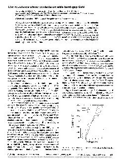
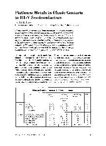
G Ivey Depart inent of Chemical and Materials Engineering Lliiiverit of A41berta Caiiada 7x10⁵ 300350 1 2 25x lo6 300 375 3 6x lob 400 450 3 4x10⁷ 400415 4 i lofi 415440 5 85x 10 440 6 6x10 450 7 4x10b 450 8 34x 10 450 9 7X1O5 420 425 10 Plulinum ID: 26107

Ivey Depart inent

Share:

Link:

Embed:

Download Presentation from below link

Download Pdf The PPT/PDF document "Platinum Metals in Ohmic Contacts to V S..." is the property of its rightful owner. Permission is granted to download and print the materials on this web site for personal, non-commercial use only, and to display it on your personal computer provided you do not modify the materials and that you retain all copyright notices contained in the materials. By downloading content from our website, you accept the terms of this agreement.


Presentation Transcript

1 x 1 x loi9 lateral uniformity. directly affected the contact. metals are semiconductors, as barriers or metallisation schemes. Examples tacts are minimum contact two types, which show rectifying current-voltage behaviour are referred the contact thus not are several for forming the most common commercial contacts layer of on the semiconductor metal, see and the field emission charge carriers may take place, giving a contact very low resistance at zero can be One method for exam- ple, by chemical vapour deposition (CVD) metal deposition. a graded contacts should in the- require subsequent annealing are there- fore referred contacts are ohmic contact Simplified plot of doping Simplified energy layered surfaces example, zinc for as a nanometres in the semiconductor by solid requires heating is usually metallisation scheme, including adhesion layers, diffusion prevent oxidation be considered probably being resistance. Several other important taken into account, contacts should be stable range, have good lateral uniformity aspects have as device dimensions are being decreased in size. However, it achieve low interdiffusion between and the compromise contact electrical properties contacts are contact resistance, the current den- a homogeneous contact contact resistance sample geometries when semiconductor substrate required for are common ponents in metallisation schemes semiconductors. Many although these contacts interface structures. based contacts less reactive more uniform inter- deposition, good oxidation resistance, relatively low reaction temperatures to the conductor) and compound formation with the Group Reactions which are summarised and platinum react with com- phases. Many phous, particularly their decomposition sections (at phase diagrams, determined bulk spec- Pd-In-P, Pt-In-P, Pt-Ga-As systems Figures 2 and three-phase region InP or phases with and Group elements. Annealing semiconductor should then in the phase region. Palladium can be to form ohmic contacts with a However, pal- in a layer metallisation, where its primary functions are to reactions with underlying semiconductor. annealing behaviour an important role in how Figure 2(a), amorphous ternary (Pd=,InP) forms ing palladium deposition ing (1 225"C, crystalline islands cubic PdJnP annealing at a continuous, thick). Two PdJnP) then form epitaxially. At Isothermal sections Isothermal sections Figure 3(a), grows epitaxially during subsequent with palladium being phase, Pd,(GaAs) higher annealing temperatures orientation relationship with GaAs. the ternary Isothermal sections ternary phase palladium metallisations subsequent formation binary compounds. PdGa and one study Pd,As were Figure 3(a), PdGa and phases in Annealing samples results in in contact with be used however, its use practice, palladium utilised as contacts, with its to the particular contact originally applied (and later see below based on regrowth mechanism this mechanism, specific case) are deposited sequentially At low annealing temperatures, semiconductor reacts with example, titanium/platinum) needed to germanium during device processing an image platinum/titanium capped sam- ple, while Figure 4(b) and deterioration uncapped sample. the ohmic con- tact until annealing complex reactions result rapid deterioration the initial decomposition been fabricated or Ge) that it and forms stable binary should also on the For the Ge/Pd- GaAs system annealing this con- ohmic behaviour cor- Pd,GaAs, which is contact resistances to 1 been achieved for GaAs, see Table. Selecting the cor- rect Ge:Pd ratio crucial for fabricat- stable contacts: Ge:Pd atomic ratio slightly exceed and this pre- the formation any excess for doping purposes. contacts to n-type GaAs, cross-section images I I cross-section micrographs Ti/Pt/Au contacts regrown InP. achieved, see Ohmic Contacts for the those for that the temperatures tend for platinum, a higher melting Ternary amorphous the formation but at layerimetallisation inter- preferred orien- in contrast where crystalline phases nucle- and then grow with preferred orientation, second ternary phases to at temperatures agree with those expected from the with PtAs, main application ohmic contacts to conductors (including InGaAs and InGaAsP) so-called non-alloyed titanium and platinum deposited either annealing, is solder bonding to a annealing permits deposition the metal reduce contact subsequent annealing. layer improves adhesion to the underlying semiconductor, acts as to a number been obtained resistance values much on the levels in semiconductors are these contacts are ohmic without or require little annealing to attain hence, the these contacts are annealed to optimise electrical properties fore undergo fairly significant interfacial reac- tions, making the terminology “non-alloyed” these contacts p-type InP, p-side metallisation used for plan view indium particles the TinnGaAs for zinc) of low contact resistances as low as been reported, microstructure development annealing are shown in dark contrast features the Ti/InGaAs interface, Figure 5(b). These been identified cles, which uniformly across interface and see Figures 5(c) and in shape grow along 1 1 planes, Figures Platinum Metals cross-section images deposited and annealed at melting point metal 57"C), which per cent and up InGaAs). Both forms at thickens with increasing anneal- ing temperature, see Figure results in gallium-rich InGaAs. annealing temperatures At higher significant interdiffusion platinum occurs. incorporate both dium and exa'mple was Figure 4(a)), although was essen- a capping some instances, platinum participate in metallisatiodsemi- shown in 7(b) for platinum reacting with type GaAs). Lateral uniformity the thin nature protects the during subsequent sputters the achieve low initial reaction between palla- and platinum and InGaP 5-component amorphous (Pd, Pt, interface. Annealing results in complete con- and partial decomposition resulting in form contact and PdGa, structure, contact are attainable. palladium are metals react with the initially, followed an adhesion major role barrier. In both palladium and platinum act hence the which they are attached. J. R. and E. Calais, J. and G. D. G. Muter. Electron., Eicher and C. Dautremont-Smith, Pearton and Trans. Electron. M. Thomas, Wan, R. to InP Materials”; Chapter Materials: Processing, Artech House, Boston, 1 2 “Silicides for Academic Press, Orlando, Florida, and R. 1987,61, 2195 G. hey, K. J. Muter. Res., Thin Solid Films, 136, 105 2 1 Sands, E. M. Murakami, “Ohmic con- and Other ed. L. Cole, L. DeAnni, K. Jones and Jian, D. Muter. Res. 1993, 300, 225 Ohmic Contacts Platinum Metals Okumura and Dve Used for example, flat-panel displays. between one electrode with and an low work source). In the presence applied electric an electron-hole exciton and mplet and the radiative recom- (singlet) exciton generates ton that as visible emitted from current trend is towards polymeric electroluminescent material processing advantages. need to the order per cent. One approach to the into the host semiconductor mater- ial. Provided the absorption spectrum emission spec- efficient energy-trans- the host to the can occur. singlet exciton states (approximately the total) tional fluorescent emission. from Princeton improved light emission A. Baldo, M. E. porphine platinum(I1) triplet exciton states to be light-emission process, conversion efficiencies up to per cent been achieved. relatively well-known as other compounds quantum and that are superior an order atom in the porphine ring increases orbit coupling the triplet state character and enhances the crossing from the enhanced light emission from to the in the triplet behaviour organic solid-state systems. International Symposium on at the Annual Meeting Metals and Materials 17th, 2000. Particular attention processing iridium compounds; coating technology; com- and applications iridium as the proceed- the symposium National Laboratory the Primary Organiser Harada, National Lanam, Engelhard-CLAL, are the co-organisers. June 15th 1999 to contact the Oak Ridge 4508, Oak Platinum Metals