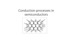
PPT-Electrical contacts to two dimensional semiconductors

Author : conchita-marotz | Published Date : 2018-10-21

Wenjin Zhao Tauno Palomaki Joe Finney Zaiyao Fei Paul Nguyen Frank McKay David H Cobden Nanodevice Physics Lab Department of Physics University of Washington Seattle

Presentation Embed Code

Download Presentation

Download Presentation The PPT/PDF document "Electrical contacts to two dimensional s..." is the property of its rightful owner. Permission is granted to download and print the materials on this website for personal, non-commercial use only, and to display it on your personal computer provided you do not modify the materials and that you retain all copyright notices contained in the materials. By downloading content from our website, you accept the terms of this agreement.

Electrical contacts to two dimensional semiconductors: Transcript


Wenjin Zhao Tauno Palomaki Joe Finney Zaiyao Fei Paul Nguyen Frank McKay David H Cobden Nanodevice Physics Lab Department of Physics University of Washington Seattle WA 981951560 2D materials . Sato and H Kata amaY oshida ISIR Osaka University 5670047 Osaka Jap an H Dederic hs IFF ese ar ch Center ulich D52425 ulich Germany Abstract describ exc hange in teractions in dilute magnetic semiconductors DMS based on abinitio calculations Electro M Sandratskii and P Bruno MaxPlanck Institut f ur Mikrostrukturphysik Weinberg 2 D06120 Halle Germany lsandrmpihallede brunompihallede Abstract We report the densityfunctionaltheory calculations of the exchange interactions and Curie temperature for G Ivey Depart inent of Chemical and Materials Engineering Lliiiverit of A41berta Caiiada 7x10⁵ 300350 1 2 25x lo6 300 375 3 6x lob 400 450 3 4x10⁷ 400415 4 i lofi 415440 5 85x 10 440 6 6x10 450 7 4x10b 450 8 34x 10 450 9 7X1O5 420 425 10 Plulinum Eric Mitchell. Acousto-Optic Modulators. Based on the diffraction of light though means of sound waves travelling though a . median. The quartz crystal has a piezoelectric transducer attached at the end that propagates strong acoustic waves within the crystal. Whether your contacts are stored in an email program, a spreadsheet, or on your phone, you’ll probably want to import them into Microsoft Dynamics CRM so you can keep track of the people you do business with all in one place.. Abstract:. 3-D ICs are particularly suited for combinations of memory with other memory or logic devices. With the integration of Through Silicon . Viasing. (TSV) for chip to chip interconnects, microelectronics manufacturers are now implementing 3-Dimensional chip stacking to improve performance, bandwidth, power, weight, and storage. . BMayer@ChabotCollege.edu. Engineering 45. Electrical. Properties-2. Learning Goals – Electrical Props. How Are Electrical Conductance And Resistance Characterized. What Are The Physical Phenomena That Distinguish Conductors, Semiconductors, . on SU(2) Group Manifold . and N=4 Gauged Supergravity. . . Patharadanai Nuchino. . Dr. Parinya Karndumri. June 8, 2016 . Room Anek, Baansuan-Khunta and Golf Resort Hotel, Ubon Ratchathani, Thailand. UK242013 Dimensional refers to the Dimensional separate but affiliated entities generally rather than to one particular entity These entities are Dimensional Fund Advisors LP Dimensional Fund Advisor Moore146s Lawstates that the number of transistors on a computer chip doubles every eighteen monthsTraditional transistors can no longer keep upToo many transistors will slow down processor speedsTran Product Manager (NXP MOTION SENSORS). NXP MEMS Manufacturing Consolidation Decision . Quality Notifications: 202009009G, 202009030DN. Motion Sensor C&I Portfolio IMPACT. Agenda. NXP MEMS Manufacturing Consolidation: Quality Notifications. A way of converting between units for problem solving. Remember all units have to be in meters, kilograms, and seconds. You can also use dimensional analysis as a way of checking your units to make sure your problem is correct. characterized. ?. • What are the physical phenomena that distinguish. conductors, semiconductors, and insulators?. • For metals, how is conductivity affected by. imperfections, temperature, and deformation?. What are Semiconductors?. Semiconductor material is a substance which has electrical conductivity between conductors and a non-conductor or insulator. Semiconductors are the core fundamental materials which are used in solid-state electronic devices such as transistors, diodes etc. The material’s atomic structure decides whether the material will turn out to be a metal, semiconductor or insulator. .

Download Document

Here is the link to download the presentation.
"Electrical contacts to two dimensional semiconductors"The content belongs to its owner. You may download and print it for personal use, without modification, and keep all copyright notices. By downloading, you agree to these terms.

Related Documents