PDF-Unpackaged Die and Wafer Storagehttp://www.national.com/en/die/appsnot
Author : celsa-spraggs | Published Date : 2016-08-22
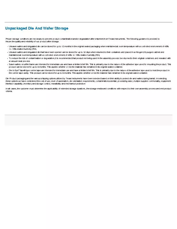
Proper storage conditions are necessary to prevent product contamination andor degradation after shipment from National Semiconductor Corp The following guidance
Presentation Embed Code
Download Presentation
Download Presentation The PPT/PDF document "Unpackaged Die and Wafer Storagehttp://w..." is the property of its rightful owner. Permission is granted to download and print the materials on this website for personal, non-commercial use only, and to display it on your personal computer provided you do not modify the materials and that you retain all copyright notices contained in the materials. By downloading content from our website, you accept the terms of this agreement.
Unpackaged Die and Wafer Storagehttp://www.national.com/en/die/appsnot: Transcript
Download Rules Of Document
"Unpackaged Die and Wafer Storagehttp://www.national.com/en/die/appsnot"The content belongs to its owner. You may download and print it for personal use, without modification, and keep all copyright notices. By downloading, you agree to these terms.
Related Documents