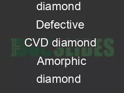
/
Defect-free Ultra-Rapid Polishing/Thinning of Diamond Crystal Radiator Targets for Highly Defect-free Ultra-Rapid Polishing/Thinning of Diamond Crystal Radiator Targets for Highly

Defect-free Ultra-Rapid Polishing/Thinning of Diamond Crystal Radiator Targets for Highly - PowerPoint Presentation

cheryl-pisano
cheryl-pisano . @cheryl-pisano
Follow
370 views
Uploaded On 2018-03-18

Defect-free Ultra-Rapid Polishing/Thinning of Diamond Crystal Radiator Targets for Highly - PPT Presentation

PI Arul Arjunan Sinmat Inc Rajiv Singh University of Florida Richard Jones University of Connecticut Program Manager Manouchehr Farkhondeh SBIR STTR Exchange Meeting Gaithersburg August 67 2014 ID: 655797

2014 sttr gaithersburg august sttr 2014 august gaithersburg meeting exchange diamond sbir crystal ray phase microns grad laser thickness

Share:

Link:

Embed:

Download Presentation from below link

Download Presentation The PPT/PDF document "Defect-free Ultra-Rapid Polishing/Thinni..." is the property of its rightful owner. Permission is granted to download and print the materials on this web site for personal, non-commercial use only, and to display it on your personal computer provided you do not modify the materials and that you retain all copyright notices contained in the materials. By downloading content from our website, you accept the terms of this agreement.


Presentation Transcript

Slide1

Defect-free Ultra-Rapid Polishing/Thinning of Diamond Crystal Radiator Targets for Highly Linearly Polarized Photon Beams

PI: Arul ArjunanSinmat Inc Rajiv SinghUniversity of FloridaRichard JonesUniversity of ConnecticutProgram Manager: Manouchehr Farkhondeh

SBIR / STTR Exchange Meeting, Gaithersburg, August 6-7, 2014

DOE STTR #DE-SC-0004190Slide2

Application: high-energy polarized photon source

uniqueness of diamond as a radiatorcompeting specifications: thickness vs. flatnessproposed solution: a thick frame around the radiator Two approaches investigatedvapor phase ion etching with mask (Sinmat)milling by UV laser ablation (UConn) Conclusions and Future Directions

Outline

SBIR / STTR Exchange Meeting, Gaithersburg, August 6-7, 2014 1 Slide3

Diamond - a high-energy polarized photon source

SBIR / STTR Exchange Meeting, Gaithersburg, August 6-7, 2014 2 Top View

7

6

m

Electron beam dump

Coherent Bremsstrahlung

9

GeV

polarized

photon beam

GlueX

detector

Collimator

Photon

b

eam

dump

Counting

House

Radiator

Pair

Spectrometer

Tagger

12 GeV

electron beam

Crystalline radiator => electrons “bremsstrahlung” from entire planes of atoms at a time

discrete peaks in energy spectrum

photons are polarized within the peaks

Diamond is the unique choice for crystal radiator

low atomic number

dense atomic packing

high thermal conductivity

radiation hard, mechanically robust, large-area monocrystals, ...Slide4

Coherent bremsstrahlung beam propertiesBremsstrahlung spectrum with (black) and without (red) an oriented diamond crystal radiatorSame spectrum, after cleanup usingsmall-angle collimationSBIR / STTR Exchange Meeting, Gaithersburg, August 6-7, 2014 3 Slide5

Diamond radiator requirements

SBIR / STTR Exchange Meeting, Gaithersburg, August 6-7, 2014 4

crystal appears as a

mosaic of microscop

ic

quasi-perfect domains

Actually includes other kinds of effects

distributed strain

plastic deformation

Measured directly by X-ray diffraction: “rocking curves”

thickness 10

-4

radiation lengths ~ 20 microns

“mosaic spread” of the crystal planes ~ 20 μrad RMSSlide6

SBIR / STTR Exchange Meeting, Gaithersburg, August 6-7, 2014 5

E6 single-crystal CVD(!) diamondVery close to theoretical rocking curve RMS width for diamond !but…These crystals are 300 microns thick.X-ray measurements performed at Cornell High Energy Synchrotron Source (CHESS)Slide7

SBIR / STTR Exchange Meeting, Gaithersburg, August 6-7, 2014 6

E6 CVD diamond thinned to 15 microns(1,0,0)(0,1,0)X-ray measurements performed at Cornell High Energy Synchrotron Source (CHESS) - STTR phase 1Sample was thinned using proprietary Sinmat RCMP process (presented in early talk)very fragile -- notice the corner broken offrocking curve shows very large bending deformation Slide8

Primary R&D challenge in Phase 2

Understand and overcome the thin diamond warping problem.SBIR / STTR Exchange Meeting, Gaithersburg, August 6-7, 2014 7 Diamonds appear to warpseverely when thinned to20 microns.T

ry to stiffen the diamond by

leaving a thick outer frame

around the 20 micron region.

F

rame around 20 micron window is still part

of

the single crystal,

acts like a drum head.

W

arping is from combination of

mounting and internal stresses.Slide9

Two-prong method of attack

Chemical etching using a mask - SinmatStep 1: Deposit a metallic mask covering the outer frame region.Step 2: Etch masked sample using oxygen VPIE.Monitor removal rates, expect >50 microns/hr Watch when mask sputters away, when gone return to step 1.Step 3: Measure central thickness, remove residual mask when done.2. Precision milling with a UV laser - UConnNew ablation facility built at UConn for this project5W pulsed excimer laser generates 5W at 193

nm

UV optics to expand beam, focus to 0.1mm spot

evacuated ablation chamber with tilted sample

holder

3D motion controls to raster the diamond across the

beam

Software developed to generate smooth flat ablated surface

SBIR / STTR Exchange Meeting, Gaithersburg, August 6-7,

2014

8 Slide10

APPROACH

1: Chemical etchingSBIR / STTR Exchange Meeting, Gaithersburg, August 6-7, 2014 9 Slight misalignment shows 4 masks were needed.Frame thickness is 185 micronsCentral region is 55 microns thickEtched surface shows significant roughness, pits 10 microns deepCareful monitoring needed to prevent burn-through below 50 μmSlide11

Diamond 2um Al using sputter metal cover mask

Diamond

2um Al using Sputter

Diamond

RIE/ICP etching

Diamond

e

tching

r

ecipe

Gases O2 & Ar gas RIE/ICP= 500W / 1500W

Vapor Phase Etch Process

SBIR / STTR Exchange Meeting, Gaithersburg, August 6-7, 2014 Slide12

Etch rate continuously reduced with progressive etchingAl mask re-sputtered on the sample80umVapor Phase Etch ProcessSBIR / STTR Exchange Meeting, Gaithersburg, August 6-7, 2014 11 Slide13

APPROACH

2: Laser ablationSBIR / STTR Exchange Meeting, Gaithersburg, August 6-7, 2014 12 200 microns removed in 8hrsurface roughness < 1 μmrisk of burn-through below 50 μm thicknessSlide14

Uniform sample S90surface and thickness profiles (Zygo 3D)SBIR / STTR Exchange Meeting, Gaithersburg, August 6-7, 2014 13Slide15

Uniform sample S30Final polish with RCMP techniqueSBIR / STTR Exchange Meeting, Gaithersburg, August 6-7, 2014 14 Slide16

X-ray assessment: S90

whole-crystal rocking curve (220)not as flat as S150, butstill in spec.SBIR / STTR Exchange Meeting, Gaithersburg, August 6-7, 2014 15 Slide17

X-ray assessment: S30 rocking curve of S30 Sinmatchallengelies here!SBIR / STTR Exchange Meeting, Gaithersburg, August 6-7, 2014 16 Slide18

X-ray diffraction: S

200_50352µrad rmsSBIR / STTR Exchange Meeting, Gaithersburg, August 6-7, 2014 17 result: large bending strain across crystalSlide19

X-ray

diffraction: UC300_40excellent result for thinned diamond!surface was not treated after ablationSBIR / STTR Exchange Meeting, Gaithersburg, August 6-7, 2014 18 Slide20

Next steps: large-area 7x7 mm

2SBIR / STTR Exchange Meeting, Gaithersburg, August 6-7, 2014 19 excellent crystal qualityvery large thickness 1.2mmSlide21

Summary of Methodsparametersmethod20 µm thicknesscut ratemultiple samplequalityReactive CMP✓

x

V

apor Phase Etch

p

rocess

x

Laser

a

blation

x

x

SBIR / STTR Exchange Meeting, Gaithersburg, August 6-7,

2014

20 Slide22

Plan: combine the 2 approaches1.2mmVPIE870µmremoved330µm

RCMP

30µm removed

300µm

Sent to UConn

300µm

20µm

Laser

Ablation

280µm

removed

SBIR / STTR Exchange Meeting, Gaithersburg, August 6-7, 2014 21Slide23

Summary

Developed a three-step process to thin diamond samplesStep 1: Vapor phase etching process (75 micron/hr)Step 2: Polish surface defects with RCMP processStep 3: Cut thin central window using laser ablationValidated results of all proposed steps using X-ray diffractionDesigned a custom diamond diffraction setup at CHESSOptimized procedures to obtain 3 rocking curves per hour

Developed analysis code to assess X-ray diffraction

topograph

Developed custom analysis code for 2-surface

profilometry

Expected by Phase 2 completion

3 production-quality crystals 7x7 mm

2

with 20 micron window

draft publication for NP instrumentation journal

SBIR / STTR Exchange Meeting, Gaithersburg, August 6-7,

2014

22 Slide24

Acknowledgements

UConn studentsBrendan Pratt (grad)Igor Senderovich (grad)Fridah Mokaya (grad)Alex Barnes (grad)Liana Hotte (undergrad)University of Florida studentsJinhyung Lee (grad)Jong Cheol Kim (grad)Minfei

Xue

(grad)

Nathan Sparks

- Catholic UniversityKen Finkelstein

-

CHESS staff and collaborator

SBIR / STTR Exchange Meeting, Gaithersburg, August 6-7, 2014 23

This work was supported by the United States Department of Energy through STTR award number DE-SC0004190, and by the National Science Foundation through grant number 1207857.

This work is based upon research conducted at the Cornell High Energy Synchrotron Source (CHESS) which is supported by the National Science Foundation and the National Institutes of Health/National Institute of General Medical Sciences under NSF award DMR-1332208

.