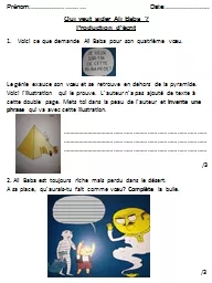
/
Dr. Ali Abadi          Chapter Three: Crystal Imperfection Dr. Ali Abadi          Chapter Three: Crystal Imperfection

Dr. Ali Abadi Chapter Three: Crystal Imperfection - PDF document

conchita-marotz
conchita-marotz . @conchita-marotz
Follow
399 views
Uploaded On 2016-06-13

Dr. Ali Abadi Chapter Three: Crystal Imperfection - PPT Presentation

1 A perfect crystal with every atom of the same type in the correct position does not exist There always exist crystalline defects which can be point defects occurring at a single lattice po ID: 361220

1 A perfect crystal with every

Share:

Link:

Embed:

Download Presentation from below link

Download Pdf The PPT/PDF document "Dr. Ali Abadi Chapter Three: Cr..." is the property of its rightful owner. Permission is granted to download and print the materials on this web site for personal, non-commercial use only, and to display it on your personal computer provided you do not modify the materials and that you retain all copyright notices contained in the materials. By downloading content from our website, you accept the terms of this agreement.


Presentation Transcript

1 Dr. Ali Abadi Chapter Three: Crystal Imperfection Materials Properties A perfect crystal, with every atom of the same type in the correct position, does not exist . There always exist crystalline defects , which can be point defects occurring at a single lattice point; line defects occurring along a row of atoms; or planar defects occurring over a two - dimensional surface in the crystal. There can also be three - dimensional defects such as voids . Crystalline Defects : Imperfections or defects: Any deviation from the perfect atomic arrangement in a crystal is said to contain imperfections or defects. Or a crystalline defect is a lattice irregularity having one or more of its dimensions on the order of an atomic dimension. There are 4 major categories of crystalline defects:  Zero dimensional: Point defects occurring at a single lattice point  One dimensional: Linear defects (dislocations) occurring along a row of atoms  Two dimensional: Planar (surface) defects occurring over a two - dimensional surface in the crystal  Three dimensional: Volume (bulk) (void) defects Defects influence the electrical and mechanical properties of solids; in fact it is the defects that are usually responsible for the existence of useful properties. While is it perhaps intuitive to think of defects as bad things, they are in fact necessary, even crucial, to th e behavior of materials: Almost, or perhaps all, technology involving materials depends on the existence of some kind of defects. Adding alloying elements to a metal is one way of introducing a crystal defect. Crystal imperfections have strong influence u pon many properties of crystals, such as strength, electrical conductivity and hysteresis loss of ferromagnetism. Thus some important properties of crystals are controlled by as much as by imperfections and by the nature of the host crystals.  The conductiv ity of some semiconductors is due to entirely trace amount of chemical impurities.  Color, luminescence of many crystals arise from impurities and imperfections 2  Atomic diffusion may be accelerated enormously by impurities or imperfections  Mechanical and pla stic properties are usually controlled by imperfections Crystal Defects Classification: 1 . Point defects: a . Vacancy b . Schottky c . Self interstitial d . Frenkel e . Colour centers f . Polarons g . Excitons 2 . Line defects a . Edge dislocation b . Screw dislocation 3 . Surface defects a . Grain boundaries b . Ti lt boundaries c . Twin boundaries d . Stacking faults 4 . Volum e defects a . Inclusions b . Voids Point Defects: Point defects are where an atom is missing or is in an irregular place in the lattice structure. Vacancies A perfect crystal with regular arrangement of atoms can not exist. There are always defects, and the most common defects are point defects. This is especially true at high temperatures when atoms are frequently and randomly change their positions leaving b ehind empty lattice sites, called vacancies . Or Vacancies are empty spaces where an atom should be, but is missing. In most cases diffusion (mass transport by atomic motion) - can only occur because of vacancies. How many vacancies are there? The higher is the temperature, more often atoms are jumping from one equilibrium position to another and larger number of vacancies can be found in a crystal. Actually, the equilibrium number of vacancies, Nv, increases expone ntially with the absolute temperature, T, and can be estimated using the equation (Boltzmann Distribution): N v = N exp( - Q v /kT) 3 Where N is the number of regular lattice sites, k is the Boltzmann constant (1.38 x 10 - 23 J/atom.K) , and Q v is the energy needed to form a vacancy in a perfect crystal. Using this simple equation we can estimate that at room temperature in copper there is one vacancy pe r 10 15 lattice atoms, whereas at high temperature, just below the melting point (1358 K) the re is one vacancy for every 10,000 atoms. These are the lower end estimations, a large numbers of additional vacancies can be introduced in a growth process or as a result of further treatment (plastic deformation, quenching from high temperature to the am bient one, etc.). A Schottky defect is a type of vacancy in which an atom being free from regular site , migrates through successive steps and eventually settles at the crystal surface. a pair of anion and cation vacancies. 4 I mpurities :  A pure metal consisting of only one type of atom just isn’t possible; impurity or foreign atoms will always be present, and some will exist as crystalline point defects.  In fact, even with relatively sophisticated techniques, it is difficult t o refine metals to purity in excess of 99.9999%. At this level, on the order of 10 22 to 10 23 impurity atoms will be present in one cubic meter of material.  Metals which have impurity called alloys.  alloying is used in metals to improve mechanical strength and corrosion resistance  The addition of impurity atoms to a metal will result in the formation of a solid solution and/or a new second phase, depending on the kinds of impurity, their concentrations, and the temperature of the al loy.  Several terms relating to impurities and solid solutions deserve mention. ( solute and solvent )  “Solvent” represents the element or compound that is present in the greatest amount host atoms .  “Solute” is used to denote an element or c ompound present in a minor concentration. Solid Solutions:  A solid solution forms when, as the solute atoms are added to the host material, the crystal structure is maintained, and no new structures are formed.  If two liquids, soluble in each other (such as water and alcohol) are combined, a liquid solution is produced as the molecules intermix, and its composition is homogeneous throughout.  A solid solution is also compositionally homogeneous; the impurity atom s are randomly and uniformly dispersed within the solid.  Impurity point defects are found in solid solutions, of which there are two types:  S ubstitutional : solute or impurity atoms replace or substitute for the host atoms  Interstitial .  There are several features of the solute and solvent atoms that determine the degree to which the former dissolves in the latter, as follows: 1 . Atomic size factor . Appreciable quantities of a solute may be accommodated in this type of solid solution only when the dif ference in atomic radii between the two atom types is less than about. Otherwise the solute atoms will create substantial lattice distortions and a new phase will form. 2 . Crystal structure . For appreciable solid solubility the crystal structures for metals o f both atom types must be the same. 5 3 . Electronegativity . The more electropositive one element and the more electronegative the other, the greater is the likelihood that they will form an intermetallic compound instead of a substitutional solid solution. 4 . Valences . Other factors being equal, a metal will have more of a tendency to dissolve another metal of higher valency than one of a lower valency. Interstitials – atoms that are squeezed in between regular lattice sites. If the interstitial atom is of the same species as the lattice atoms, it is called self - interstitial . Creation of a self - interstitial causes a substantial distortions in the surrounding lattice an d costs more energy as compared to the energy for creation of a vacancy ( Q i � Q V ) and, under equilibrium conditions, self - interstitials are present in lower concentrations than vacancies . Foreign, usually smaller atoms (carbon, nitrogen, hydrogen, oxygen) are called interstitial impurities. Interstitial impurity atoms are much smaller than the atoms in the bulk matrix. Interstitial impurity atoms fit into the open space between the bulk atoms of the lattice structure. An example of interstitial impurity ato ms is the carbon atoms that are added to iron to make steel. Carbon atoms, with a radius of 0.071 nm, fit nicely in the open spaces between the larger (0.124 nm) iron atoms . They introduce less distortion to the lattice and are more common in real materials and more mobile. If the foreign atom replaces or substitutes for a matrix atom, it is called a substitutional impurity . A substitutional impurity atom is an atom of a different type than the matrix atoms, which has replaced one of the bulk (matrix) atoms in the lattice. Substitutional impurity atoms are usually close in size (within approximately 15%) to the bulk atom. An example of substitutional impurity atoms is the zinc ato ms in brass. In brass, zinc atoms with a radius of 0.133 nm have replaced some of the copper atoms, which have a radius of 0.128 nm. 6 Example: Calculate the equilibrium number of vacancies per cubic meter for copper at 1000 o C . The energy for vacancy formation is 0.9 eV/atom; the atomic weight and density (at 1000 O C) for copper are 63.5 g/mol and 8.4 g/cm3, respectively. A Frenkel defect is a pair of cation (positive ion) vacancy and a cation interstitial. Or it may also be an anion (negative ion) vacancy and anion interstitial. Or the combination of a vacancy and interstitial is called a Frankel defect. However anions are much larger than cations and it is not easy for an anion interstitial to form. In both Frenkel and Schottky defects, the pair of point defects stays near each other because of strong coulombic attraction of their opposite charges. Specification of Composition:  It is often necessary to express the composition (or concentration ) of an alloy in terms of its constituent elements.  two most common ways to specify composition 7 1 . weight (or mass) percent (wt%) is the weight of a particular element relative to the total a lloy weight. For an alloy that contains two hypothetical atoms denoted by 1 and 2, the concentration of 1 in wt%, C 1, is defined as C 1 = 1 1 + 2 × 100% …………….. (1) Where m 1 and m 2 represent the weight (or mass) of elements 1 and 2, respectively C 2 = 2 1 + 2 × 100% 2 . A tom percent (at%) calculations is the number of moles of an element in relation to the total moles of the elements in the alloy. The number of moles in some specified mass of a hypothetical element 1, n m1 , may be computed as follows: n m1 = 1 1 ……………… (2) Where, 1 and A 1 denote the mass (in grams) and atomic weight, respectively, for element 1. Concentration in terms of atom percent of element 1 in an alloy containing 1 and 2 atoms, 1 ! is defined by : In like manner, the atom percent of 2 may be determined.  Atom percent computations also can be carried out on the basis of the number of atoms instead of moles, since one mole of all substances contains the same number of atoms. 8 Composition Conversions Sometimes it is necessary to convert from one composition scheme to another ; for example, from weight percent to atom percent. We will now present equations for making these conver sions in terms of the two hypothetical elements 1 and 2. Using the convention of the previous section (i.e., weight percents denoted by C 1 and C 2 atom percents by 1 ! and 2 ! and atomic weights as A 1 and A 2 ), these conversion expressions are as follows: Conversion of weight percent to atom percent (for a two - element alloy) Conversion of atom percent to weight percent (for a two element alloy) Since we are considering only two elements, computations involving the preceding equations are simplified when it is realized that In addition, it sometimes becomes necessary to convert concentration from weight percent to mass of one component per unit volume of material (i.e., from units of wt% to kg/m 3 ); this latter composition scheme is often used in diffusion c omputations. Concentrations in terms of this basis will be denoted using a double prime (i.e., 1 " and 2 " ), and the relevant equations are as follows: Conversion of weight percent to mass per unit volume (for a two element alloy) 9 For density in units of g/cm 3 , these expressions yield 1 " and 2 " in kg/m 3 . Furthermore, on occasion we desire to determine the density and atomic weight of a binary alloy given the composition in terms of either weight percent or atom percent. If we represent alloy density and atomic weight by ρ ave and A ave respectively, then Computation of density (for a two element metal alloy) Computation of atomic weight (for a two element metal alloy) 10 Example: Determine the composition, in atom percent, of an alloy that consists of 97 wt% aluminum and 3 wt% copper. If we denote the respective weight percent compositions as C Al =97 and C Cu =3, substitution into Equations 4 and 4 - a yields 11 Colour centers: Atomic and electronic defects of various types which produce optical absorption bands in otherwise transparent crystals such as the alkali halides, alkaline earth fluorides, or metal oxides. They are general phenomena found in a wide range of materials. Color centers are produced by gamma radiation or x - radiation, by addition of impurities or excess constituents, and sometimesthrough electrolysis . Polarons: When a charge carrier (an electron or hole) is placed into a solid, the surrounding ions can interact with it ( e.g. , positive ions will be slightly attracted to a negatively charged carrier). The ions can adjust their positions slightly, balancing their interactions with the charge carrier and the forces that hold the ions in their regular places. This adjustment of po sitions leads to a polarization locally centered on the charge carrier. The induced polarization will follow the charge carrier when it is moving through the medium. The combo of the carrier + the surrounding polarization is a polaron. Excitons: An exciton is a bound state of an electron and hole which are attracted to each other by the electrostatic Coulomb force . It is an electrically neutral quasiparticle that exists in insulators , semiconductors and some liquids. The exciton is regarded as an elementary excitation of condensed matter that can transport energy without transporting net electric charge 12 Linear Defects (Dislocations) : In linear defects groups of atoms are in irregular positions. Linear defects are commonly called dislocations. Any deviation from perfectly periodic arrangement of atoms along a line is called the line imperfection. A line defect is a lattice distortion created about a line formed by the solidification process, plastic deformation, vacancy condensation or atomic mismatch in solid solutions. The line imperfection acting as boundary between the slipped and un - slipped region, lies in the slip plane and is called a dislocation. Dislocations are generated and move when a stress is applied. The strength and ductility of metals are controlled by dislocations. T w o extreme types of dislocations are distinguish as 1. Edge dislocations and 2. Screw dislocations. 13 Edge Dislocations: The inter - atomic bonds are significantly distorted only in the immediate vicinity of the dislocation line. As shown in the set of images below , the dislocation moves similarly a small amount at a time. The dislocation in the top half of the crystal is slipping one plane at a time as it moves to the right from its position in image (a) to its position in image (b) and finally image (c). In the process of slipping one plane at a time the dislocation propagates across the crystal. The movement of the dislocation across the plane eventually causes the top half of the crystal to move with respect to the bottom half. However, only a small fraction of the bonds are broke n at any given time. Movement in this manner requires a much smaller force than breaking all the bonds across the middle plane simultaneously. Edge dislocation is considered positive when compressive stresses present above the dislocation line, and is represented by ┴. If the stress state is opposite i.e. compressive stresses exist below the dislocation line, it is considered as negative edge dislocation, and represented by ┬. A schematic view of edge dislocations are shown in figure below. 14 Screw Dislocations: The screw dislocation is slightly more difficult to visualize. The motion of a screw dislocation is also a result of shear stress, but the defect line movement is perpendicular to direction of the stress and the atom displacement, rathe r than parallel. To visualize a screw dislocation, imagine a block of metal with a shear stress applied across one end so that the metal begins to rip. This is shown in the upper left image. The lower left image shows the plane of atoms just above the rip. The atoms represented by the blue circles have not yet moved from their original position. The atoms represented by the red circles have moved to their new position in the lattice and have reestablished metallic bonds. The atoms represented by the green c ircles are in the process of moving. It can be seen that only a portion of the bonds are broke at any given time. As was the case with the edge dislocation, movement in this manner requires a much smaller force than breaking all the bonds across the middle plane simultaneously. If the shear force is increased, the atoms will continue to slip to the right. A row of the green atoms will find their way back into a proper spot in the lattice (and become red) and a row of the blue atoms will slip out of positio n (and become green). In this way, the screw dislocation will move upward in the image, which is perpendicular to direction of the stress. Screw dislocation or Burgers dislocation has its dislocation line parallel to the Burger’s vector. A screw dislocation is like a spiral ramp with an imperfection line down its axis. Screw dislocation is considered positive if Burger’s vector and t - vector or parallel, and vice versa. ( t - vector – a unit vector representing the direction of the dislocation line). A positive screw dislocation is represented by a dot surrounded by circular direction in clock - wise direction”, whereas the negative screw dislocation is represented by a dot surrounded by a circular direction in anti - clock - wise direction”. A schematic view of a negative screw dislocation is shown in right image in above figure. 15 Dislocations more commonly originate during plastic deformation, during solidification, and as a consequence of th ermal stresses that result from rapid cooling Interfacial defects Interfacial defects can be defined as boundaries that have two dimensional imperfections in crystalline solids, and have different crystal structures and/or crystallographic orientations on either side of them. They refer to the regions of distortions that lie about a surface having thickness of a few atomic diameters. For example: external surfaces, grain boundaries, twin boundaries, stacking faults, and phase boundaries. These imperfections are not thermodynamically stable, rather they are meta - stable imp erfections. They arise from the clustering of line defects into a plane. External surface: The environment of an atom at a surface differs from that of an atom in the bulk; especially the number of neighbors (coordination) at surface is less. Thus the un saturated bonds of surface atoms give rise to a surface energy. This result in relaxation (the lattice spacing is decreased) or reconstruction (the crystal structure changes). To reduce the energy, materials tend to minimize, if possible, the total surface area. Grain boundaries: Crystalline solids are, usually, made of number of grains separated by grain boundaries. Grain boundaries are several atoms distances wide, and there is mismatch of orientation of grains on either side of the boundary as shown in figure below . When this misalignment is slight, on the order of few degrees (10°), it is called low angle grain boundary . These boundaries can be described in terms of aligned dislocation arrays. If the low grain boundary is formed by edge dislocations, it is called tilt boundary , and twist boundary if formed of screw dislocations. Both tilt and twist boundaries are planar surface imperfections in contrast to high angle grain boundaries. For high angle grain boundaries , degree of disorientation is of lar ge range �( 15°). Grain boundaries are chemically more reactive because of grain boundary energy. In spite of disordered orientation of atoms at grain boundaries, polycrystalline solids are still very strong as cohesive forces present within and across the boundary. At ambient temperatures, grain boundaries give strength to a material. So in general, fine grained materials are stronger than coarse grained ones because they have more grain boundaries per unit volume. However, at higher temperatures, grain boundaries act to weaken a material due to corrosion and other factors. 16 Twin boundaries: It is a special type of grain boundary across which there is specific mirror lattice symmetry. Twin boundaries occur in pairs such that the orientation change introduced by one boundary is restored by the other ( figure below ). The region between the pair of boundaries is called the twinned region. Twins which forms during the process of recrystallization are called annealing twins , whereas deformation twins form during plastic deformation. Twinning occurs on a definite crystallographic plane and in a speci fic direction, both of which depend on the crystal structure. Annealing twins are typically found in metals that have FCC crystal structure (and low stacking fault energy), while mechanical/deformation twins are observed in BCC and HCP metals. Annealing tw ins are usually broader and with straighter sides than mechanical twins. Twins do not extend beyond a grain boundary. 17 Stacking faults: They are faults in stacking sequence of atom planes. Stacking sequence in an FCC crystal is ABC ABC ABC …, and the sequence for HCP crystals is AB AB AB…. When there is disturbance in the stacking sequence, formation of stacking faults takes place. Two ki nds of stacking faults in FCC crystals are: (a) ABC AC ABC…where CA CA represent thin HCP region which is nothing but stacking fault in FCC, (b) ABC ACB CABC is called extrinsic or twin stacking fault . If the HCP structure is going along as ABABAB and sudd enly switches to ABABABCABAB, there is a stacking fault present Volume Dislocations: Volume defects as name suggests are defects in 3 - dimensions. These include pores, cracks, foreign inclusions and other phases. These defects are normally introduced duri ng processing and fabrication steps. All these defects are capable of acting as stress raisers, and thus deleterious to parent metal’s mechanical behavior. However, in some cases foreign particles are added purposefully to strengthen the parent material. T he procedure is called dispersion hardening where foreign particles act as obstacles to movement of dislocations, which facilitates plastic deformation. The second - phase particles act in two distinct ways – particles are either may be cut by the dislocatio ns or the particles resist cutting and dislocations are forced to bypass them. Strengthening due to ordered particles is responsible for the good high - temperature strength on many super - alloys. However, pores are detrimental because they reduce effective l oad bearing area and act as stress concentration sites. Atomic vibrations: Atomic vibrations occur, even at zero temperature (a quantum mechanical effect) and increase in amplitude with temperature. In fact, the temperature of a solid is really just a measure of average vibrational activity of atoms and molecules. Vibrations disp lace transiently atoms from their regular lattice site, which destroys the perfect periodicity. In a sense, these atomic vibrations may be thought of as imperfections or defects. At room temperature, a typical vibrational frequency of atoms is of the order of 10 13 vibrations per second, whereas the amplitude is a few thousandths of a nanometer. Many properties and processes in solids are manifestations of this vibrational atomic motion. For example: melting occurs once the atomic bonds are overcome by vigor ous vibrations.