/
Crystal Imperfection Crystal Imperfection

Crystal Imperfection - PowerPoint Presentation

danika-pritchard
danika-pritchard . @danika-pritchard
Follow
482 views
Uploaded On 2017-05-05

Crystal Imperfection - PPT Presentation

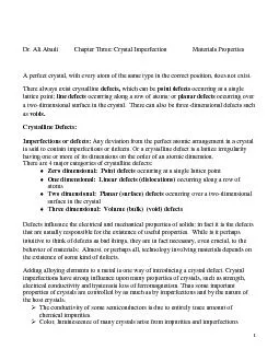
Crystals Basis with infinite space lattice Infinite periodicity Real crystals are finite in extent Therefore they have surface at boundary where some atomic bonds are broken Surface itself is an imperfection ID: 544909

crystal dislocation imperfections edge dislocation crystal edge imperfections called vacancy atoms atom vacancies defects boundary stacking void surface imperfection burgers boundaries line

Share:

Link:

Embed:

Download Presentation from below link

Download Presentation The PPT/PDF document "Crystal Imperfection" is the property of its rightful owner. Permission is granted to download and print the materials on this web site for personal, non-commercial use only, and to display it on your personal computer provided you do not modify the materials and that you retain all copyright notices contained in the materials. By downloading content from our website, you accept the terms of this agreement.


Presentation Transcript

Slide1

Crystal Imperfection

Crystals:

Basis with infinite space lattice. Infinite periodicity.

Real crystals:

are finite in extent. Therefore, they have surface at boundary where some atomic bonds are broken. Surface itself is an imperfection.

In addition, there are other occasional disruption in periodicity within a crystal. Volume wise disruption may be 0.01%.Slide2

Why we bother for imperfection

The study of imperfections has a two fold purpose, namely,

A better understanding of crystals and how they affect the

properties of metals.

Exploration of possibilities of minimizing or eliminating these

defects.

The term

“defect”

or

“imperfection”

is generally used to

describe any deviation from the perfect periodic array of

atoms in the crystal. Slide3

Why we bother for imperfection

PROPERTIES

Structure sensitive

Structure Insensitive

E.g. Yield stress, Fracture toughness

E.g. Density, elastic modulusSlide4

Classification of Imperfection

On the basis of geometry

POINT

IMPERFECTIONS

LINE IMPERFECTIONS

SURFACE IMPERFECTIONSVOLUME IMPERFECTIONSSlide5

POINT IMPERFECTIONS

They are imperfect point- like regions, one or two

atomic diameters in size and hence referred to as

‘zero dimensional imperfections’.

There are different kinds of point imperfections.

VACANCIES

If an atom is missing from its normal site in the

matrix, the defect is called a

vacancy defect

.

It may be a single vacancy,

divacancy

or a

trivacancy

. Slide6

Missing atom from an atomic site

Atoms around the vacancy displaced

Tensile stress field produced in the

vicinity

A pair of one cation and one anion can be missed from an ionic crystal. Such a pair of vacant ion sites is called Schottky imperfection.

Vacancy

Tensile Stress

Fields ?

SCHOTTKY IMPERFECTIONSSlide7

Impurity

Interstitial

Substitutional

SUBSTITUTIONAL IMPURITY

Foreign atom replacing the parent atom in the crystal

 E.g.

Cu sitting in the lattice site of FCC-Ni INTERSTITIAL IMPURITY

Foreign atom sitting in the void of a crystal

 E.g.

C

sitting in the octahedral void in HT FCC-

Fe

Compressive stress fields

Tensile Stress

Fields

Compressive

Stress

Fields

Relative

sizeSlide8

Interstitial

C

sitting in the octahedral void in HT FCC-

Fe

rOctahedral void / rFCC atom

= 0.414 rFe-FCC = 1.29 Å 

rOctahedral void = 0.414 x 1.29 = 0.53 Å rC

= 0.71 Å

 Compressive strains

around the C atom Solubility limited to 2 wt% (9.3 at%)

Interstitial

C

sitting in the octahedral void in LT BCC-

Fe

r

Tetrahedral

void

/

r

BCC

atom

= 0.29

r

C

= 0.71

Å

r

Fe

-BCC = 1.258 Å  r

Tetrahedral void = 0.29 x 1.258 = 0.364 Å► But C sits in smaller octahedral void- displaces fewer atoms

 Severe

compressive strains around the C atom

Solubility limited to 0.008

wt% (0.037 at%)Slide9

ENTHALPY OF FORMATION OF VACANCIES

Formation of a vacancy leads to missing bonds and distortion of the

lattice

The potential energy (Enthalpy) of the system increases

Work required for the formaion of a point defect

Enthalpy of formation (Hf) [

kJ/mol or eV / defect] Though it costs energy to form a vacancy its formation leads to

increase in configurational entropy

 above zero Kelvin there is an equilibrium number of vacancies

Crystal

Kr

Cd

Pb

Zn

Mg

Al

Ag

Cu

Ni

kJ / mol

7.7

38

48

49

56

68

106

120

168

eV / vacancy

0.08

0.39

0.5

0.51

0.58

0.70

1.1

1.24

1.74Slide10

G = H  T S

G (putting n vacancies) = nH

f

 T Sconfig

Let n

be the number of vacancies, N the number of sites in the lattice Assume that concentration of vacancies is small i.e. n/N << 1 

the interaction between vacancies can be ignored

Hformation (n vacancies) = n . Hformation (1 vacancy) Let H

f

be the enthalpy of formation of 1 mole of vacancies

S = S

thermal

+ S

configurational

zero

For minimum

Larger contributionSlide11

Considering only configurational entropy

User

R

instead of

k

if

H

f

is in J/mole

Assuming n << N

Using

S = S

thermal

+ S

configurational

Independent of temperature, value of ~3

?Slide12

T (

ºC)

n/N

500

1 x 10

10

1000

1 x 10

5

1500

5 x 10

4

2000

3 x 10

3

H

f

= 1 eV/vacancy

= 0.16 x 10

18

J/vacancy

G (perfect crystal)

Certain equilibrium number of vacancies are preferred at T > 0K

At a given TSlide13

13

Estimate number of vacancies in Cu at room T

k

B

= 1.38

10-23 J/atom-K = 8.62  10-5 eV/atom-K

T = 27o

C + 273 = 300 K. k

BT = 300 K  8.62  10-5 eV/K = 0.026 eV

Q

v

= 0.9

eV

/atom

N

s

= N

A

/

A

cu

N

A

=

6.023

10

23 atoms/mol

 = 8.4 g/cm3

Acu = 63.5 g/molSlide14

Ionic Crystals

Overall electrical neutrality has to be maintained

Frenkel defect

Cation (being smaller get displaced to interstitial voids

E.g. AgI, CaF

2Slide15

ELECTRONIC DEFECTS

Errors in charge distribution in solids are called

electronic defects

’.

These defects are produced when the composition of an ionic crystal does not correspond to the exact

stoichiometric formula.

These defects are free to move in the crystal under

the influence of an electric field.Slide16

Other defects due to charge balance

If Cd

2+

replaces Na

+

→ one cation vacancy is created

Defects due to off stiochiometry

ZnO heated in Zn vapour → ZnyO (y >1)

The excess cations occupy interstitial voids

The electrons (2e

) released stay associated to the interstitial cationSlide17

FeO heated in oxygen atmosphere

→ Fe

x

O

(x <1)

Vacant cation sites are present Charge is compensated by conversion of ferrous to ferric ion: Fe

2+ → Fe3+ + e

For every vacancy (of Fe cation) two ferrous ions are converted to ferric ions → provides the 2 electrons required by excess oxygenSlide18

LINE IMPERFECTIONS

The defects, which take place due to dislocation or distortion of atoms along a line, in some direction are called as ‘

line defects

’.

Line defects are also called dislocations. In the geometic sense, they may be called as ‘one dimensional defects’.A dislocation may be defined as a disturbed region between two substantially perfect parts of a crystal.

It is responsible for the phenomenon of slip by which most metals deform plastically.Slide19

EDGE DISLOCATION

In perfect crystal, atoms are arranged in both vertical and horizontal planes parallel to the side faces.

If one of these vertical planes does not extend to the full length, but ends in between within the crystal it is called

edge dislocation

’. In the perfect crystal, just above the edge of the incomplete plane the atoms are squeezed and are in a state of compression.

Just below the edge of the incomplete plane, the atoms are pulled apart and are in a state of tension.What is the edge dislocation?Edge dislocations

. An edge dislocation is a defect where an extra half-plane of atoms is introduced mid way through the crystal, distorting nearby planes of atoms.Slide20

EDGE DISLOCATION

The distorted configuration extends all along the edge into the crystal.

Thus as the region of maximum distortion is centered around the edge of the incomplete plane, this distortion represents a line imperfection and is called an edge dislocation.

Edge dislocations are represented by ‘

’ or ‘

‘ depending on whether the incomplete plane starts from the top or from the bottom of the crystal. These two configurations are referred to as positive and negative edge dislocations respectively.Slide21
Slide22

BURGERS VECTOR

The magnitude and the direction of the displacement are defined by a vector, called the

Burgers Vector

.

In figure (a), starting from the point P, we go up by 6 steps, then move towards right by 5 steps, move down by 6 steps and finally move towards left by 5 steps to reach the starting point P.Now the Burgers circuit gets closed.

When the same operation is performed on the defect crystal (figure (b)) we end up at Q instead of the starting point.Slide23

BURGERS VECTOR

So, we have to move an extra step to return to P, in order to close the Burgers circuit.

The magnitude and the direction of the step defines the Burgers Vector (BV).

BV = = b

The Burgers Vector is perpendicular to the edge dislocation line.Slide24
Slide25

Video of Edge Dislocation

https://www.youtube.com/watch?v=-t6btGjGKYUSlide26

SCREW DISLOCATION

In this dislocation, the atoms are displaced in two separate planes perpendicular to each other.

It forms a spiral ramp around the dislocation.

The Burgers Vector is parallel to the screw dislocation line.

Speed of movement of a screw dislocation is lesser compared to edge dislocation. Normally, the real dislocations in the crystals are the mixtures of edge and screw dislocation.Slide27

SCREW DISLOCATIONSlide28

Video address for screw dislocationhttps://www.youtube.com/watch?v=TxJOP3hA6ToSlide29

SURFACE IMPERFECTIONS

Surface imperfections arise from a change in the stacking of atomic planes on or across a boundary.

The change may be one of the orientations or of the stacking sequence of atomic planes.

In geometric concept, surface imperfections are two- dimensional. They are of two types external and internal surface imperfections.Slide30

EXTERNAL SURFACE IMPERFECTIONSSlide31

GRAIN BOUNDARIESSlide32

TILT BOUNDARIES

This is called low-angle boundary as the orientation difference between two

neighbouring

crystals is less than 10°.

The disruption in the boundary is not so severe as in the high-angle boundary. In general low-angle boundaries can be described by suitable arrays of dislocation.

Actually a low-angle

tilt boundary

is composed of edge dislocation lying one above the other The angle or tilt will be

where

b = Burgers vector and D = the average vertical distance between dislocations.Slide33

TILT BOUNDARIESSlide34

TWIN BOUNDARIES

If the atomic arrangement on one side of a boundary is a mirror reflection of the arrangement on the other side, then it is called as

twin boundary

.

As they occur in pair, they are called twin boundaries. At one boundary, orientation of atomic arrangement changes.

At another boundary, it is restored back. The region between the pair of boundaries is called the twinned region.

These boundaries are easily identified under an optical microscope. Slide35
Slide36

STACKING FAULTS

Whenever the stacking of atomic planes is not in a proper sequence throughout the crystal, the fault caused is known as

stacking fault

.

For example, the stacking sequence in an ideal FCC crystal may be described as A-B-C-A-B-C- A-B-C-……. But the stacking fault may change the sequence to A-B-C-A-B-A-B-A-B-C. The region in which the stacking fault occurs (A-B-A-B) forms a thin region and it becomes HCP.

This thin region is a surface imperfection and is called a stacking fault.Slide37
Slide38

VOLUME IMPERFECTIONS

Volume defects such as cracks may arise in crystals when there is only small electrostatic dissimilarity between the stacking sequences of close packed planes in metals. Presence of a large vacancy or void space, when cluster of atoms are missed is also considered as a volume imperfection.

Foreign particle inclusions and non crystalline regions which have the dimensions of the order of 0.20 nm are also called as volume imperfections.Slide39

Physics is hopefully simple but Physicists are not