PPT-Supplement on Verilog
Author : danika-pritchard | Published Date : 2018-01-20
Sequential circuit examples FSM Based on Fundamentals of Digital Logic with Verilog Design and Fundamental of Logic Design ChungHo Chen 1 A Simple Circuit Using
Presentation Embed Code
Download Presentation
Download Presentation The PPT/PDF document "Supplement on Verilog" is the property of its rightful owner. Permission is granted to download and print the materials on this website for personal, non-commercial use only, and to display it on your personal computer provided you do not modify the materials and that you retain all copyright notices contained in the materials. By downloading content from our website, you accept the terms of this agreement.
Supplement on Verilog: Transcript
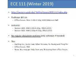
Sequential circuit examples FSM Based on Fundamentals of Digital Logic with Verilog Design and Fundamental of Logic Design ChungHo Chen 1 A Simple Circuit Using Blocking Assignment 2 At . Verify the analog/digital interfaces at block and SoC levels. Check properties involving voltages and currents. Check complex timing constraints that don’t fall on digital clock boundaries. Verify analog IP and their correspondence with behavioral models. SPECIAL SUPPLEMENT SPECIAL SUPPLEMENT Nursing Times Deteriorating Patient Supplement When patients come into hospital they put their trust in the professionals caring for them. They assume they are be 數位電路實驗. TA: . 吳柏辰. Author: Trumen. Outline. Environment . Setup. NC-Verilog. nLint. nWave. Verdi. 2. Environment Setup. 3. Login to the Linux Server. Many EDA tools . are . provided only for . Coding in Verilog. Lecturer:. Simon Winberg. Digital Systems. EEE4084F. module . myveriloglecture. ( . techniques_out. , . wishes_in. );. … . // implementation of today’s lecture. …. Navneet. . Vidyarthi. CHAPTER 14 SUPPLEMENT . Linear Programming. OPERATIONS MANAGEMENT. : . Creating Value Along the Supply Chain, . Canadian . Edition. Lecture Outline. Model Formulation. Graphical Solution Method. Montek Singh. Aug 29, 2014. Topics. Hierarchical Design. Verilog Primer and Advanced. 2. Design Hierarchy. Just like with large program, to design a large chip need hierarchy. Divide . and Conquer. To create, test, and also to understand. 3/8/2017. Objectives. Learn to write Verilog for a custom design. Understand how to verify your design using functional simulation . Learn to write Verilog test bench for your design . Run Length Encoding. Hardware Description Language. 3/8/2015. 1. Hwk4: see your email/. ublearns. a. b. c. d. e. f. g. 3/8/2015. 2. Hardware Description Language. 3/8/2015. 3. A HDL is a computer based language that describes the hardware of digital systems in a textual form.. Professor Bill Lin. Office hours: . Wed 1:00-1:50p, . 4310 Atkinson Hall. Lectures:. Section A00: . MW 2:00-3:20p. , . EBU1-2315. Section B00: . MW . 3:30p-4:50p, . EBU1-2315. No . regular discussion sections . . Office of Federal Programs. Oklahoma State Department of Education. 405-521-2846. Title I Supplement not Supplant. ESSA Section 1118 (b). (1) In General - A State educational agency or local educational agency shall use Federal fund received under Title I only to supplement the funds that would, in the absence of such Federal funds, be made available from State and local sources for the education of students participating in programs assisted under Title I, and not supplant such funds.. (Brief) Introduction to Verilog. Acknowledgement. The slides used in this set contain material/illustrations from Prof. Milo Martin, Andy Phelps, Altera tutorial on HDL basics, Prof. Stephen brown and Prof. Steve Wilton.. Cavendish Nutrition is the best dietary supplement manufacturer, protein manufacturer, capsule manufacturer, immune system supplement and liquid contract manufacturer service provider in New York. Contact us for your all melatonin manufacturers, quercetin manufacturers, collagen peptides manufacturer, vitamin d manufacturers, anxiety supplement manufacturers, elderberry private label supplements organic manufacturer needs. 1 th Gr de ThinkStretch, llc | ww w. thinkstretc h . com STOP WINTER BRAIN FREEZE Help Brain and Professor have winter fun! For every day you read, add an item to the snow globe. GRA ) HE staining of healthy bone of . a humanized mouse. . Asterisk (*) . indicates . fibrotic area . in . bone marrow. Magnification 5x. . *. *. A. *. B. Supplement . 2. : . Bone turnover was analyzed by measuring serum levels of PINP, CTX and the ratio of PINP/CTX. (upper row). Quantitation of number of .
Download Document
Here is the link to download the presentation.
"Supplement on Verilog"The content belongs to its owner. You may download and print it for personal use, without modification, and keep all copyright notices. By downloading, you agree to these terms.
Related Documents