/
APPLICATION NOTE APPLICATION NOTE

APPLICATION NOTE - PDF document

ellena-manuel
ellena-manuel . @ellena-manuel
Follow
387 views
Uploaded On 2016-07-18

APPLICATION NOTE - PPT Presentation

AN0971 OneTechnologyWayPOBox9106Norwood02062USA Recommendations for Control of Radiated Emissions with isoPower DevicesMark Cantrell 
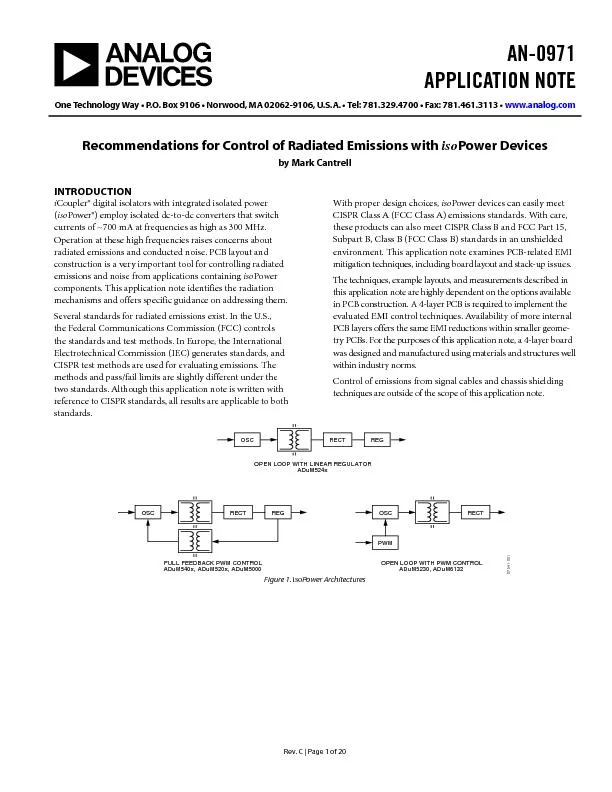
Rev Page of NTRODUCTIONCoupler ID: 409190

AN0971 OneTechnologyWayP.O.Box9106Norwood 02062U.S.A. Recommendations for Control Radiated

Share:

Link:

Embed:

Download Presentation from below link

Download Pdf The PPT/PDF document "APPLICATION NOTE" is the property of its rightful owner. Permission is granted to download and print the materials on this web site for personal, non-commercial use only, and to display it on your personal computer provided you do not modify the materials and that you retain all copyright notices contained in the materials. By downloading content from our website, you accept the terms of this agreement.


Presentation Transcript

AN0971 APPLICATION NOTE OneTechnologyWayP.O.Box9106Norwood,02062U.S.A. Recommendations for Control of Radiated Emissions with isoPower DevicesMark Cantrell ��Rev. | Page of NTRODUCTIONCoupler®digital isolators with integrated isolated power Poweremploy isolated toconverters that switch currents of ~700at frequencies as high as 300 MHz. Operation at these OSC REG RECTOPEN LOOP WITH LINEAR REGULATORADuM524x OSC REG RECT FULL FEEDBACK PWM CONTROLADuM540x, ADuM520x, ADuM5000 OSC PWM RECTOPEN LOOP WITH PWM CONTROLADuM5230, ADuM613207541-001 Figure isoower Architectures Application Note ��Rev. | Page of TABLE OF CONTENTSIntroductionRevision HistoryisoPower OverviewSources of Radiated EmissionsEdge EmissionsInputOutput Dipole EmissionsSources of Conducted NoiseEMI Mitigation TechniquesInputOutput StitchingEdge GuardingInterplane Capacitive BypassingPower ReductionOperating VoltageRecommended Design PracticesMeeting Isolation StandardsEvaluating PCB Structures for EMIEdge Guarding ResultsOperating Load and Voltage DependenceInterplane CapacitanceIntegrating TechniquesExample 1Basic Insulation BoardExample 2Reinforced Insulation BoardAdditional Layout ConsiderationsConclusionsReferencesREVISION HISTORY1/14Revto Rev. Added Table 1 and changeto and moved Power Overview SectionChange to Edge Emissions SectionChanges to EMI Mitigation TechniquesSectionChange to Equation 2anges to Interplane Capacitive BypassingSection/11Rev. A to Rev. B Changes to Introduction Section, isoPower Overview Section, and Figure 1Changes to Edge Emissions Section and InputOutput Dipole Emissions SectionAdded Figure 3; RenumberedSequentiallyChanges to Sources of Conducted Noise SectionDeleted Figure 9; Renumbered SequentiallyChanges to EMI Mitigation Techniques Section and InputOutput Stitching SectionAdded Safety Rated Capacitor Sectionand Stitching Capacitance Built into the PCB SectionAdded Floating Capacitive Structure Section and Gap Overlap Stitching SectionReplacedFigure 6andFigure 7Changes toEdge Guarding SectionDeleted Figure 13Deleted Table 2; Renumbered SequentiallyDeleted Figure 1Changes to Figure 9 and Figure 10Replaced Buried Capacitance Bypassing Section withInterplane Capacitive Bypassing SectionAdded Figure 11Changes toFigure 12and Power Reduction SectionReplaced Figure 13Deleted Appendix AA Design Example Section, Figure 16, and Figure 17Added Operating Voltage SectionChanges to Recommended Design Practices SectionChanges to Meeting Isolation Standards SectionAdded Figure 14Added Table 1; Renumbered SequentiallyReplaced Example Board Section withEvaluating PCB Structures for EMI SectionChanges to Figure 15Added Figure 16 and Figure 17Changes to Table 2Added Stitching Capacitance Results Section, Figure 18, and Figure 19Added Figure 20Edge Guarding Results Section, Table 3, and Figure 21Added Operating Load and Voltage Dependence Section, Figure 22, Figure 23, and InterplaneCapacitance SectionAdded Integrating Techniques Section, Figure 24, Example 1Basic Insulation Board Section, Table 4, and Figure 2Added Figure 26 Through Figure 30, Example 2Reinforced sulation Section, and Table 5Added Additional Layout Considerations Section and Figure 31Changes to Conclusions Section and References Section3/09Rev. 0 to Rev. A 6/08Revision 0: Initial Version Application Note ��Rev. | Page of isoPOWER OVERVIEThePower productshown in Table represent a significant step forward in isolation technology. AnalogDevices, Inc., has leveraged their experience inmicrotransformerdesign to creatchip scale dcdc power converters. These power converters are incorporated into Analog Devices signal isolation products. Power levels of up to onehalf watt are available, at output voltages ranging from 3.3V to 15 V. Power is used to power the secondary side of the Coupler data channels as well as to provide power to offchip loads. Because the Analog Devices standard data couplers use asimilar magnetic technology, EMI can be an issue in dataonlyCouplers and the data channels of Power devices. Emissions from data channels are addressed in the 1109 Application NoteControl of Radiated Emissions in Coupler DevicesAnalog Devices uses several power architectures to achievedesired design goals, such as efficiency, small size, and high outputvoltage (see Figure ). These architectures have three common elements: a transformer to couple power to the secondary side of the Coupler, an oscillator tank circuit that switches current into the transformer at an optimum frequency for efficient power transfer, and a rectifier that recreates a dc level on the secondary side. Several regulation methods are used in these products.The physics of the transformer requires that the oscillator circuit switch current into the transformer at a rate ranging from between 180 MHz and 300 MHz. The rectifier circuit on the secondary side effectively doubles this frequency during the rectification process. These functions are common in switching power supplies; however, the operating frequency is three orders of magnitude higher than a standard dcdc converter. Noise generated by the operation of the converter into the 30 MHz to 1 GHz range is of concern for radiated emissionsTable isoPower Products thatmay Require Steps to Control Radiated EmissionsOpenLoop with Linear RegulatorOpenLoop with Primary Side PWM ControlHigh Power Full Feedback PWM ControlLow Power Full Feedback PWM Control ADuM5240ADuM5230ADuM5000ADuM5010 ADuM5241 ADuM6132 ADuM5 200 ADuM5210 ADuM5242ADuM5201ADuM5211 ADuM5202ADuM5212 ADuM5400ADuM6010 ADuM5401ADuM6210 ADuM5402ADuM6211 ADuM5403ADuM6212 ADuM5404 ADuM6000 ADuM6200 ADuM6201 ADuM6202 ADuM6400 ADuM6401 ADuM6402 ADuM6403 ADuM6404 Application Note ��Rev. | Page of RADIATEDEMISSIONSThere are two sources of emissions in PCBs where Power is used: edge emissions and inputoutput dipole emissionsEDGE EMISSIONSEdge emissionsoccur when unintended currents meet the edges of ground anpower planes. Theseunintended currentscan originatefromGround and power noisegenerated by inadequate bypass of high power current sinks.Cylindricallyradiated magnetic fields coming from inductive viapenetrationsradiateout between board layers eventuallymeeting the board edgeStrip line image charge currents spreadingfrom high frequency signal lines routed too close to the edge of the board.Edge emissions are generated (see Figure where differential noisefrom many sources meets the edge of the boardleaking out of a planeplane spaceandacting as a wave guide GROUNDPOWER07541-002 Figure . Edge Radiation rom an Edge Matched Ground Power Pair 07541-003 GROUNDPOWERSIGNA 20hh Figure Edge RadiationFrom Edge Mismatched Power Ground PairAt the edge boundarythere are two limiting conditionsThe edges of the ground and power planes are lined upas shown in Figure or one edge is pulled back by some amountas shown in Figure . In the first case oflined up edges, there is some reflection back into the PCB and some transmission of the fields out of the PCB. In the second case, the edge of the boards makes a structure similar to the edge of a patch antenna. When the edges mismatch by where h is the plane to plane pacing, the fields couple out of the PCB very efficientlyresulting in very high emissions. These two limiting cases become important to discussions of edge treatment of the PCBINPUTTOOUTPUT DIPOLE EMISSIONSInputoutput dipole radiation is generated by driving current source across a gap betweenground planes.This is the predominant mechanism for radiationfor Power applications. Isolated power suppliesby their very naturedrive energyacross gaps in ground planes. The inability of high frequency image chargesassociated with the power signal to cross the boundary causedifferential signals across the gap driving thedipole. In many cases,this is a very large dipole as shown in Figure similar mechanismcauses high frequency signal lines to radiate when crossing splits in theground and power planeThis type of radiationis predominantly perpendicular to the gap in the ground planes. 07541-004 11689 Figure Dipole Radiation Between Input and Outputhe ADuM5400ADuM5401ADuM5402ADuM5403, and ADuM5404deviceserves good exampleof the issues involved in generating and mitigating emissions. The oscillator tank circuit in these devices runs at approximately 180MHz. It can regulate its output to either 5or 3.3V under the control of a pin on the secondary side. The input voltage can be in thto 5V range. The highest power operating mode is 5input and 5V outputand is the primaryconfiguration examined in this application noteWhen operating under a full 100mA output load, the average input current is about 290mA. This means that the peak current in the tank circuit is abouttwice that value at switching rate of MHz. Thecomponent’s bypass capacitor is supposed to provide this high frequency current locally. This is a lot of current for a bypass capacitor to handle. The capacitor must provide large charge reserves. Atthe same timethe capacitormust have a very low series resistance at 180MHz. ven with multiple low ESR capacitors near the pins, an inductively limited bypass allowsvoltage transientsand the noise is injected onto the ground and power planes.Power transfersto the output side where it is rectified into The rectification process doubles the tank frequency to 360MHz.The inputoutput emissions are bothat the rectification frequency andthe tank frequencyalong with somehigher harmonicsFigure shows worstcase data collected on a layer evaluation boardwith a near field probe. Application Note ��Rev. | Page of 07541-005 180MHz 360MHzRECTIFIER HARMONICS540MHz720MHz Figure FFT of the Near Field Emissions from a 2Layer Boardboard with near field emissionsas showin Figure and without a chassis shield would ail FCC lass B emissions standards by approximatelydB at the 360z peak. Application Note ��Rev. | Page of SOURCES OF CONDUCTEDNOISEThe large currents and frequencies also generate conducted noise on the ground and power planes. This issue is addressedalong withradiated emissions becausethe causesand remedies for both types of EMI are addressedwith the samePCB ground and power structures.he inability of the bypass capacitors and ground/power planes to provide adequate high frequency current to the Powertoconvertercauses Vnoise. The dcdc converterswitches power in bursts of 2.5pulses with an amplitude of mA. An ideal bypass capacitor of a few microfaradsshould be adequate to supply thac component of thecurrent. Real worldbypass capacitors are not idealand they connect to onemore likelybothof the power planes by an inductive via. In addition, a large distance between ground and power planes creates a large inductance between themrestricting their ability to supply current quicklyThese factors contribute to a large fraction of a volt of high frequency noise on the Vplane. Application Note ��Rev. | Page of EMI MITIGATION TECHNIQUESanymitigation techniques are available to the designer.Several techniques that apply directly to the Power devicesare identified in this sectionThe choice of how aggressivelyEMI must be addressed for a designto pass FCC/CISPRemissions levels depends on the requirements of the design as well as cost and performance tradeoffs. The easiestradiated EMI mitigation technique to implement is to place the PCB in a grounded chassis with filter elements limiting noise escapingon cable shields. Although this application note does not describethis optionnotethatwhere PCB related techniques are impractical, this method remainsavailableThe EMI mitigation practices rely on having relatively continuous ground and power planes and the ability to speciftheir relative positions and distances in the stackup. This dictates that the minimum total number of planes is three: ground, power, and signal planeFor practical considerations in board manufacture, a layer board the minimum stackup. More layers are acceptableand can be used to greatly enhance the effectiveness of the recommended techniqueshe following techniquesareeffective in reducing EMI radiation and onboard noise:Inpututput ground plane stitchingcapacitancePower control Edge guardingInterplane capacitive bypassCircuit boards with test structures were prepared to evaluate each of theseEMImitigation techniques utilizing theADuM5400ADuM5401ADuM5402ADuM5403, and ADuM5404The layout of each board was varied as little as possible to allow meaningful comparison of results. Testing was conducted at an EMI test facility in a shielded chamberAs expected, duringEMI testing, it was determinedthat the emissionsat the tank frequency (180MHz) were predominantly in the plane of the boardsuggesting that the primary mechanism for radiation is from the PCB edges. The rectificationemissions(360MHz)are primarily perpendicular to the isolation gap in the ardsuggesting inputoutput dipole radiation.INPUTTOUTPUT STITCHINGWhen current flows along PCB traces, an image charge follows along the ground plane beneath the trace. If the trace crosses a gap in the ground plane, the image charge cannot follow along. This creates differential currents and voltages in the PCB leading to radiated and conducted emissions. The solution is to provide a path for the image charge to follow along with the signal. Standard practice is to place a stitching capacitor inproximity to the signal across the split in the ground plane(see PCB Design for RealWorld EMI Controlby Archambeault and Drewniak in the Referencessection). This same technique works to minimizeradiation between ground planes due to the operation of isoPower.There are at least three options to form a stitching capacitance. A safety rated capacitor applied across the barrier.A floating metal planespanningthe gap between the isolated and nonisolated sides on an interior layeras shown in Figure Extending the ground and ower planes on an interior layer into the isolation gap of the PCB to form a capacitoras shown in Figure Each of these options has its advantages and disadvantages in effectiveness and area required to implement.Safety Rated CapacitorA stitching capacitance can be implemented with a simpleceramic capacitor across the barrier. Capacitors with guaranteed creepageclearanceand withstand voltagecan be obtained from many major capacitor manufacturerssuch as Murata, Johansen, Hitano, and Vishay. Safety rated capacitors are availablein several grades depending on their intended use. The Y2 grade is used in lineground applications where there is danger of electric shock and is the recommended safety capacitor type for a stitching capacitorin a safety rated applicationThis type of capacitor is available in surfacemount and radial leaded disk versions. Becausesafety capacitors are discretecomponents, they must be attached to the PCB with pads or through holes. This adds inductance to the capacitor on top of its intrinsic inductance. It also makes the stitching capacitor localized, demanding that currents flow to the capacitor, which can create asymmetrical image charge paths and added noise. These factors limitthe effectiveness of discrete capacitors to frequencies below about MHz.Stitching Capacitance Built into the PCBThe PCB itself can be designed to create a stitching capacitorstructure in several ways. A capacitor is formed when two planes in a PCB overlap. In this type of capacitorthe inductance of the parallel plate capacitor formed is extremely low, and the capacitance is distributed over alarge areahese structures mustbe constructed on internal layers of a PCB. The surface layers have minimum creepage and clearance requirements; therefore, it is not practical to use surfacelayers for this type of structureThis requiresminimum of four board layers.A good option is to use a floating metal structure on an interior layer of the board to bridge between the primary and secondary power planes. Note that, hereafter, planes dedicated to ground or power are referred to as reference planes because,from an ac noise pointof viewthey behave the same and can be used for stitching capacitance interchangeably. Application Note ��Rev. | Page of Floating Capacitive StructureAn example of a floating stitching capacitnce is shown inFigure The reference panes are shown in blue and greenand the floating coupling plane is shown in yellow. The capacitance of this structure creates two capacitive regions (shown with shading) linked by the nonoverlapping portion of the structure.To ensure that optimum capacitance is created for the area of the structure, the overlap areas of the primaryand secondarysides should be equal. 07541-006 w1w2Id Figure Floating Stitching CapacitanceThe capacitive coupling of the structurein Figure is calculatewith the following basic relationships for parallel platecapacitors 2121CCCCC , dCCxA21 , and hereis the toal stitching capacitanceis the overlap area of the stitching capacitanceto each reference planethethickness of the insulation layer in the PCB(see Figure is the permittivity of free space8.854 F/mis the relativepermittivity of the PCB insulation material, which is about 4.5 for FR4. 2121wwwwdlC (1)where , and are the dimensions of the overlapping portions of the floating plane and the primary and secondary reference planesas shown in Figure If the equation simplifies to dlwC21 (2)There are advantages and disadvantages of this structure in real applications. The major advantage is that there are two isolation gaps, one at the primary and one at the secondary. These gaps are called cemented joints, where the bondingbetween layers of FR4 provides the isolation. There are also two sequential paths through the thickness of the PCB material. The presence of these gaps and thicknesses is advantageous when creating a reinforced isolation barrier under some isolation standards. The disadvantage of this type of structure is that the capacitanceis formed under active circuit area so there can be viapenetrations and traces that run across the gapsEquation 2 also shows that the capacitance formed is half as effective perunit area usedcompared to a simple parallel plate capacitorThis architecture is best suited to applications where a larger amount of board area is available or were reinforced insulation is required.Gap OverlapStitchingA simple method of achieving a good stitching capacitance is to extend a reference plane from the primary and secondary sides into the area that is used for creepage on the PCB surface. 07541-007 wId Figure Overlapping Plane Stitching CapacitanceThe capacitive coupling of the structure in Figure is calculated with the following basic relationships for parallel plate capacitors dAC and (3)hereis the total stitching capacitanceis the thickness of the insulation layer in the PCB,is the permittivity of free space8.854 F/mis the relativepermittivity of the PCB insulation material, which is about 4.5 for FR4. dlwC (4)where and are the dimensions of the overlapping portion of the primary and secondary reference planesas shown in Figure The major advantageif this structure is that the capacitance is created in the gap beneath the isolator, where the top and bottom layers must remainclear for creepage and clearance reasons. This board area is not utilized at all in most designs. The capacitance created is also twice as efficient per unit area as the floating plane.This architecture has only a single cemented joint and a single layerof FR4 between the primary and secondary reference planes. It is well suited to smaller boards where only basic insulation is required.EDGE GUARDINGNoiseon the power and ground planes that reachesthe edge of a circuit board can radiate as shown in Figure andFigure If the edge is treated with a shieldingstructure, the noise is reflected back into the intplane space(see Archambeault and Drewniak in theReferencessection). This can increase the voltage noise on the planesbut reduces edge radiation. Making a solid conductive edge treatment on a PCB is possible, butthe process is expensive. A less expensive solution that Application Note ��Rev. | Page of works well is to treat the edges of the board with a guard ring structure laced together by viaThestructure is shown in Figure for a typical layerboard.Figure shows how this structure can beimplemented on the power and ground layers of the primary side of a circuit board GROUNDGROUND VIA EDGE FENCEAND GUARD RINGS07541-008 POWER Figure Via Fence Structure, Side View 07541-009 Figure Via Fence and Guard Ring, Shown on thePrimaryPower Plane LayerThere are two goals in creating edge guarding. he first is to reflect cylindrical emissionsfrom viaback into the interplane space, not allowing it to escape from the edge. The secondisto shieldany edge currents flowing on internal planes due to noise or large currents.The spacing of the viaused to create the edge guard is difficult to determine without extensive modeling. Analog evicestest boards used 4mm viaspacing for theevaluation boards. This spacing is small enough to provide attenuation to signals less than 18GHz, and it conformed to generalguidance from other sources. The number of viarequired is reasonable. Further investigation into the viadensity was not conducted. INTERPLANECAPACITIVEBYPASSINGInterplanecapacitance bypassing is a techniqueintended to reduce both the conducted and radiatedemissions of the board by improving the bypass integrity at high frequenciesThis has two beneficial effects.First,it reduces the distance that high frequency noise can spread in theground anpower planepairecondit reduces the initial noise injected into the power ground planes by providing bypass capacitance that is effective between 2MHz and 1GHz(see Archambeault and Drewniak in the Referencessection)Power and ground noisereduction providesa better operating environment for noise sensitive components near the Power device.onducted missions arereduced proportionate to the reduction in power and ground noise. reductionin radiated emissionsis not as significant as that achieved with the stitching or edge guarding techniques;however, significantlyimproves thepowerenvironment of the boardThe stackused for EMI test boardswas signalgroundpowersignalas shown in Figure thincore layer used for thepower and ground planes.These tightly coupled planes provide the nterplanecapacitance layerthat supplements the bypass capacitors required for proper operation of the device GROUNDPOWERSIGNAL/POWERBURIEDCAPACITIVELAYERSIGNAL/GROUND07541-010 Figure 10PCB tackp for InterplaneCapacitanceIn addition to the ground and power planes, the capacitance can be increased even further by filling signal layers with alternating ground and power fill. The top and bottom layers in Figure are labeled signpower and signalground to illustratethe fills on those particular layers. This has the added benefit of creating additional shielding for EMI that leaks around the edges of a viafence structure, keeping it in the PCB.Care must be taken when making ground and power fills. These fills must be tied back to the full reference planebecausea floating fill can act as a patch antenna and radiate instead of shielding.Some recommended practices for fills includeFills should be tied to their appropriate reference plaalong the edges with viaevery 10mm. Thin fingers of fill should be removedIf the fill has an irregular shape, put viaat the extreme edges of the shape 07541-0 POWER FILLGROUNDEDVIA FENCEVIA TO REFERENCEPLANE AVOID SMALLFILL ISLANDS Figure 11Features of FillThe effectiveness of nterplanecapacitance is shownFigure It shows the noise generated by the PWM controlling the primary side oscillator in apart such as the ADuM5000or a similar parts in that series (see Table for a parts list). In the top section is the noise on the Vpin generated in a 2layer board. The center section shows a substantial improvement in PCB with ground and power planes separated by 24mil. Finally, in the lower pane, a tightly spaced ground and power plane with mil separation showsnoise much smaller than the supplyripple. Application Note ��Rev. | Page of 2-LYER BOARD NO POWER PLANE 24MIACING BETWEEN POWERAND GROUND 4MIACING BETWEEN POWERAND GROUND Δ460mV Δ104mV Δ64mV07541-012 Figure 12Voltage Noise for Various StackUp OptionsPOWER REDUCTIONIn Power devices with active feedback architecture, emissions can be reduced by keeping the tank circuit off as longas possible. Running Power with light loads achieves this for the deviceslisted in Table ad reduction proves to be a very significant factor in emissions levels.OPERATING VOLTAGEThe perating voltage is the last parameter to choose when designing with isoPower. It is not as straightforward as simply selectinga lowpoweror lovoltage operating condition. As shownin Figure the emissions at 180MHZ correlateclosely with the duty factor of the PWM regulationsignaland are largely independent of operating voltage. The PWM duty factor controls the proportion of time that the tank oscillator is actively switching. It implies that the noise generated by the tank circuit (180MHz peak) is not directly proportionalto the average current. 3.3VPWM DUTY FACTOR (%)EMISSIONS (dBµV/m)07541-013 Figure 13Emissions at the 180MHz nk Frequency vs. PWM Duty FactorEmissions at 360MHz is proportionalto theaverage load current. In practical application, this means that choosing whether it is better to operate at 3.3V or 5V from an EMI point of view depends on which peak needs to be controlledand the required load current. See the Operating Load and Voltage Dependencesection of this application note for additionalinformation Application Note ��Rev. | Page of RECOMMENDED DESIGN RACTICESConsider the following general design practicefor minimizing EMI issues on PCBs. These methods do not introduce any additional isolation boundaries in the PCB that need certification review.Use a stackup ofat leastfourlayers.Spacethe powerandgroundplaneas closelyas practical to optimize bypass.All viain the power path should be as large as practical. Small viahave high inductance and generate noise. Using multiple small viais not as effective in reducing viainductance as a single large viabecausethe bulk of the current goes through the closest via, even if multiple paths are present.Be very careful to routsignal lines against a single reference plane. It is vital to maintain the image charge path so that imagecharges do not have to travel by circuitousroutesto meet back with the original signal on another plane.Do not routhighspeed linelose to the edges of the PCB.Routing data or power offboard, especially through cablescan introduce an additional radiation concern.Feedthroughfilter capacitors osimilar filter structures can be used to minimize cable radiation. Application Note ��Rev. | Page of INGISOLATION TANDARDShe techniques describedin this application note do not ffect board isolation, with the exception ofinputoutput coupling through a stitching capacitance. When stitching is implemented with a safety capacitor, the capacitor hasrated working and transient voltagesas well as specified creepage and clearance. This makes the safety capacitorrelatively easy to deal with from a certification point of view.However, its performance as an EMI suppression element is limited.he PCBstitching capacitor, byits natureis most effectivewhen conductors are located asclose to each other as possible.obtainmaximum performance from these elementsit is necessary to push the internal spacing requirements as close to the limitas possible, while maintaining safety. Differentstandards can havecompletely different approaches to PCBconstructionand the applicable standard must be appliedCertification agencies treat the surface layers of a multilayer PCB differently than interior layers. The surface hascreepage and clearance requirements that are driven by air ionization and reakdown along dirty surfaces. Interior layers are treated as solid insulation or permanently cemented joints between solid insulation. CREEAGE/CLEARANCECEMENTEDJOINT07541-014THROUGHINSUL Figure 14Critical Distances in PCB DesignIn PCB insulation, it is important to certification agencies that materials have an adequate dielectric breakdown to pass the transient test requirements and that they are constructed in a way that the insulation does not break down over time. Table compares four standardswhat is required to make a basic or reinforced insulation barrier inside a PCB.In the case of basic insulation in printed circuit boards, there is no minimum specification for distance through the insulation. Thus, the designer has a great deal of flexibility in board layout. Materials such as FR4 must be thick enough to withstand the required overvoltage for the life of the product.einforced insulation requiresa minimum distance of 0.4 mm (about 16 mil) of insulation along a bonded surface, such as the gap between copper structures on an internal PCB layer or directly through the insulation from layer to layerin most casesIn addition, there can be type testing requirements for circuit boards unless multiple layers of insulation are used between active structures. Although this requirement necessitates careful board design and possibly more thanfour layers, it should not be burdensome if taken into account at the start of a design. Capacitive coupling across the isolation barrier allows ac leakage and transients to couple from one ground plane to the other. Although 300 pF seems small, high voltage, high speed transients can inject significant currents across the barrier through this capacitance. Take this into account if the applicationis to be subjected to these environments.Table Comparison of Isolation Creepage in Isolation Standards IEC 60950IEC 61010 2nd EditionIEC 61010 3rd EditionIEC 60601 Type of InsulationThrough nsulation (2.10.6.4) Along a emented oint (2.10.6.3) Through nsulation (6.7.2.2.3) Along a Cemented Joint(6.7.2.2.3) Through nsulation (6.7) Along a Cemented Joint(6.7) Cemented and Solid Insulation Functional Insulation No requirement No requirement No requirement No requirement0.4 mm minimum 0.4 mm minimum Verified by test Basic InsulationNo requirementNo requirementNo requiremenNo requirement0.4 mm minimum0.4 mm minimumVerified by test Supplemental/Reinforced insulation0.4 mm minimum or multiple layers of insulation, precured0.4 mm minimum (2.10.5.2)No requirementNo requirement0.4 mm minimum or multiple layers of insulation, precured0.4 mm minimumVerified by test Application Note ��Rev. | Page of EVALUATING PCB STRUCTURES FOR EMIChoosing a combination of PCB structures and techniques can achieve the desired system radiated EMI goal. There are two sets of standards for radiated emissions, one from the United States Federal Communications Commission (FCC) and a second from Comité Internationale Spécial des Perturbations Radioelectrotechnique (CISPR), a special committee of the IEC. FREQUENCY (MHz)EMISSIONS LIMITS (dBµV/m)07541-015 FCC CLASS BFCC CLASS ACISPR 22 CLASS BCISRR 22 CLASS A Figure 15. FCC and CISPR Limits Corrected to 10 m Antenna DistanceIn this application note, the CISPR22 emissions standards are used for evaluating the PCB results. Figure shows therelationshipbetween FCC and CISPR levels. Over most of thespectrum, the CISPR levels are more conservative than the FCC levels, and because many products for the international markets must address both standards, only the CISPR pass limits are referenced in this application note. Refer to Figure for therelevant FCC levels if they are required for analysis.Effectiveness of the EMI mitigation techniques was verified by creating a set of evaluation boards with different combinations of stitching capacitance, edge guarding, and size. The control for these experiments was a 4layer PCB with interior ground and power planes separated by 4 mil of FR4. This gives a goodamount of interplane capacitance on each side of the boundary, no edge guarding, and no stitching capacitance, as shown in Figure . Testing was conducted at an EMI facility in a 3 m screen room. The goal was to viewthe broad spectrum of emissions rather than to focus on individual peaks. Peaks from this test correlate well to the results from the 10 m far field results. 07541-016 Figure 16Control BoardReferring to Figure , the emissions at these frequencies must be below 30 dBµV/m at 180 MHz and below 37 dBµV/m at MHz normalized to 10 m antenna distance to achieve assB emissions levels. The configuration of the control board is considered a standard PCB layout for isolation application. Emissions at a 5 V operating condition and full load represent the worst case for radiated emissions. Figure shows the facility data collected for the control board. The features to note are the tank frequency peak at 180 MHz and the rectification frequency of 360 MHz. The harmonics at higher frequencies usually disappear when EMI mitigation is applied. 07541-017FIELD STRENGTH CORRECTED TO 10m (dBµV/m)360MHz 180MHz 720MHz 540MHzEMISSIONS FREQUENCY (MHz) 900MHz Figure 17Emissions from the Control Board V and 90%Load Application Note ��Rev. | Page of Table shows that emissions from this board are significant and must be reduced by 32dB for the 360MHz peak and 3dB for the 180 MHz peak to bringtheminto compliance with CISPR Class B. Reducing that dB of emissions is the goal of thedesign.In the Stitching Capacitance Resultsand Edge Guarding Resultssections, the data presentedis normalized to the 5V/5V 90% load condition with no stitching capacitance, so that values from Figure Figure Figure and Table can be subtracted from the baseline operation of the application board directly.Table . Class B Emission LimitsRequirements180 MHz360 MHz Layer PCB Emissions Class B Limit Required EMI Reduction Stitching Capacitance ResultsThe addition of stitching apacitance has proven to be the most effective way to reduce emissions across the entire spectrum. It is most effective when it has very low inductance and is spread across theentire length of the barrier. The optimum geometry to achieve a level of stitching capacitance is dependent onavailable space and requirements of the regulatory requirements controlling the design. For this evaluation,a gap overlap capacitance was implemented becauseit developsa large capacitanceand s a part of the PCB that is usually cleared of all traces and components. Several other options are available and are describedin the Integrating Techniquessection.gure shows the PCB layout with the internal planesoutlined. The board is built on a 4 mil core withpower and groundplanes extending from each side to overlap in the middle. The overlap is lmm by wmm and the separation0.1mm. Applying Equation 4the stitching capacitance ispF. An additional PCB was made with a shorter ength to generatepF of stitching capacitance.A modification allowed pF capacitancemeasurementsas well.An example data set is shown in Figure . The peaks canclearly be seen at the expected frequencies. The two curves representthe control board with no stitching capacitance and the 300pF overlap stitching capacitor configuration. There is a dramatic 25dB to dB drop inemissions due to the stitching capacitance depending on the peak. The peak values vary with load and voltage, but the reductions are independent of operating voltage and load current. 07541-018 Figure 18Overlap Stitching Capacitance 07541-019EMISSIONS (dBµV/m)FREQUENCY (MHz) NO STITCHING300pF STITCHING igure 19Effect of 300pF of Stitching Capacitance on Emissions of a 10% Loaded ADuM540or Similar DeviceFigure summarizes the emissions as a function of stitching capacitance. Note that the shape of the curves is dependent on the frequency range of the emissions peak. Lower frequency emissions(200MHz)are only slightly reduced until thecapacitance is greater than 150pF. Higher frequency emissions (&#x-900;200MHz) have the majority of their reduction at less than 150pF. Application Note ��Rev. | Page of STITCHING CAPACITANCE (pF)EMISSIONS (dBµV/m)07541-020 180MHz 360MHz Figure 20Reduction in Emissions Due to Stitching Capacitance for 5 V/Operation at 10% LoadThe difference in the shape of the curves seemsto be primarily related to inductance in the capacitive coupling and therequired amount of capacitance to achieve the optimum result. At MHz the low inductance stitching has sufficiently coupled the input and output planes with 150pF. The 180MHz emsions are primarily from the input plane and more bulk capacitance is required to reduce emissions. This makes some options availablebecausemost component capacitors are still very effective as bypass below 200MHz, the stitching capacitance can be made from a combination of PCB based stitching for low inductance and discrete component capacitors to increase the total capacitance. Several examples of options are examined in the Integrating TechniquessectionThe shape of the curves shows that whenthe amount of stitching capacitance is limited due to available board space, other measures must be taken to reduce the low frequency emissions, such as adding component capacitancor edge guarding.EDGE GUARDING RESULTIn wer systems, the bulk of the current flows in the primary side ground and power planes and the vias that connect them to the active pins. This results in the majorityof the edge radiation occurring on the primary side.dge guarding is most effective when applied tothe planes of the primary side of the converter. Figure illustrates adding edge guarding to the test vehicle. Table Edge Guarding Reduction in EmissionsBoard TypeMHzMHZ Edge Guard  11 dB µ V/m  4.5 dB µ V/m 07541-021 Figure 21Overlap Stitching CapacitanceEdge Guardingand Ground/Power FillsGuarding is installed on both sidesbut it is lesseffective on the secondary planes.guard ring was applied each layer, except the reference layer (see Figure and Figure and the layers linked together with vias every 4mm. There are a few options for fencing near the Coupler. If spacing is tight, the fence can e interrupted on all layers under the deviceas shown in Figure Guard ringscan also be interrupted only on the top and bottom layersand can continue on interior layers. The more disruption there is in the edge fencethe more EMI leakage is possible.somesystemisolation requirements, there can be a large distance required along cemented joints, up to the full surface creepage. In these casesstitching and edgeguarding is still possible and even more desirable. If long internal PCB creepage is required, in many casesthe stitching capacitance structures appear very similar tothe offset edge case shown inFigure which can bean efficient radiatorAn example of using edge guarding for offset edges is shown in Figure Results for the edge guarded board are presented in Table Becausemost of the edge emissions are generated on the primary side by the large primary side currents, he largest ductions are in the 180MHz peak, typically aboutV/mThe results for the 360MHz peak areless than half as large Application Note ��Rev. | Page of OPERATING LOAD AND VOLTAGE DEPENDENCEmissions are directly related to the length of time the tank oscillator is on. Figure and Figure showhow emissions at the tank frequency and the rectification frequency vary with load. The emissions are nearly linear with the currentat higher loadshe emissions drop significantly at very light loadswhere the tank circuit may not turn on completely. With both light load and low output voltage, it is possible to reduce tank and rectification emissions by over 20 dB.Because of therelationship of the ank uty actor to the load current at different voltages, the 180MHz radiation when operating at 60mA and3.3loadcontains as much energy as operating at 100mA and 5see Figure . Howeverthe power transferred at 5V is more than twice as high. 0.020.040.060.080.10ISO CURRENT (A)EMISSIONS (dBµV/m)07541-0223.3V Figure 22issions180MHz vsLoad CurrentWhen the 360MHz behavior is examined in Figure it behaves more as expected with the 3.3V emissions lower over almost the entire operating range. There is a significant benefit to running at 3.3V atlow load conditions. 0.020.040.060.080.10ISO CURRENT (A)EMISSIONS (dBµV/m)07541-0233.3V Figure 23Emissions at 360MHz vs. Load CurrentWhen comparing the 180 MHz and 360 MHz responses atdifferent voltages, these results show that operating at3.3V and low load, there is only a smallpenalty at 180MHzand a benefit at MHz. If there is a high load current, it is best to run at 5INTERPLANECAPACITANCEThe use of interplanecapacitance in these designs has a marginal effect on emissions but a significant effect on power supplynoise. The same layers used for stitching capacitance also make nterplanecapacitance on each side of the barrier. The same characteristicsthat producegood coupling for a stitchingcapacitance also makegood nterplanecapacitancehat isthin layers and continuous planes.The boardshownin Figure has alternating ground and power fills implemented in unusedsections of signal layers. This can add to the nterplanecapacitance and has no effect on isolation. The islands of fill are connected to their respective planes with vias every 10mm, and the layout is careful to avoid fingers of fill or isolated islands.Use of signal layers in high layer count boards can also allow increased stitching capacitance by interdigitation of multiple layers(see the Integrating Techniquessection for additional information) Application Note ��Rev. | Page of INTEGRATINGECHNIQUESeterminingexactly which of the methods describedin this application note should be combinedto achieve the emissions targetrequires an expected baseline emissions measurementThe behavior of the control board can be used ifno other estimate is available.any of the options do not have a largeimpact on cost or area and canbe implemented on any multilayer PCB. The process of choosing the PCB layout and application techniques to minimize EMI is illustrated in Figure . This breaksthe process downinto three categoriesitemsthat do not affect isolation, iems that have isolation impacts, andfinallysystem level approachsuch as shielding 07541-024 STEPSO MINIMIZEisoPOWER EMIMINIMIZE LOADREINFORCEDBASICEDGE GUARDING3.3V OPERBURIEDSYSTEMSHIELDING TINGSTITCHING OVERLAPPINGSTITCHINGSAFETSTITCHING SAFETSTITCHING MEDICAAPPLICTION? PROTECTIONLEVE THESE FETURESIMPLEMENTEDWITH MINIMACOSTAND BOARDACT ONISOLTION.THESE FETURESCAN IMISOLTINGS.SYSTEMSHIELDINGIS UNDESIRABLEIN MOSTCASES. Figure 24Selecting EMI Mitigation Options To illustrate this process, two examples areexaminedwhichcover most aspects of the process. To start with, create two types f application boards.A PCB capable of 60 mA of average current that must meet basic insulationA PCB that supplies less than 10 mA of currentbut is capable of reinforced insulationThe control board used as thebaseline. Its emissions at full load are shown in Table along with the CISPR Class B limits. EXAMPLE 1BASIC INSULATION BOAFor the first layout example, the 60mA load is assumed to be the maximum loadrequired for the applicationThis reducethe emissions by several decibelswithout any design effort. However, becausethis isstillrelativelyheavy current applicationfrom an Power perspectiveedge guarding of theprimary side is recommendedEdge guardingreducethe 180MHz peak by 10and providesome reduction of the 360MHz peak as well. In addition, with the large power requirement, choosing a V/5V operating condition givethe lowest emissions (see Figure ). Optimizing nterplanecapacitance should beconsidered if there are sensitive analog circuits or long cables attached to the application PCB, but it is optional.The emissions have been reducdB to dB from the baseline with the methods already usedbut to obtainthe 32dB and 36dB reductions required for Classstitching capacitancemust be employedBecause this is not a medical application, the user has theflexibility to addcross barrier capacitanceOnlybasic insulation is required; thereforethe smallestsize of the stitching capacitor is the single overlapoption. Adding up the reductions thusfar yields 15dB in the 180MHz peak and dB in the 360MHz peak. This leaves 17dB in the lower frequency and 21dB at the higher frequency to obtain. As shown inFigure140pF of stitchingis requiredto achieve the goal for the 360MHz peak, but 250is required to make the 180MHz peak meet the desired level. Using Equation 4, assuming a 4 mil dielectric and an 8mm overlap,mm long capacitorstructureis required to produce a 250 pF capacitanceTable Basic Insulation 4Layer BoardRelativeChange ParameterValueMHz MHz Peak Power LevelmA at 5V/mV/m Edge GuardingN/AV/mV/m StitchingV/mV/m TotalV/mV/m Table shows a summary of the reductions achieved with a pF stitching capacitance with edge guarding anmA of current at 5V. The capacitive stitch is built as shown in Figure Note thatwith a layerboard, the full PCB creepage must be observed on the top and bottom layers, but the spacingcan be much smaller onthe internal layers. 07541-025 SIGNAL/GND FILSURACE CREEAGEPWRGNDSIGNAL/PWR FIL CEMENTED JOINTS Figure 25Basic Insulation Single Overlap Stitching Capacitor Application Note ��Rev. | Page of This design may acceptable if 77mm of overlap lengthis available. If space is at a premium, an additional optionshown in Figure Becausethe required capacitance for the MHz peak is smaller than what is required at 180MHz, design the PCB for the 140pF stitching capacitance and supplement with a safety rated capacitor. This reducethe length of the stitching capacitor to mm andadda 160pF safety capacitor. 07541-026 SIGNAL/GND FILPWRGNDSIGNAL/PWR FIL Figure 26Augmented Stitching with Safety CapacitorFinally, Figure shows the basic insulation structure with edge guards in place. Note that the ground planes used for the edge guard are also used for the stitching capacitor. This avoids the 20h patch antenna effect. 07541-027 SIGNAL/PWR FILGNDPWRSIGNAL/GND FILSIGNAL/GND FILPWRGNDSIGNAL/PWR FIL Figure 27Edge Guarding Added to the Basic Capacitive StitchingAn additional technique to increase capacitance without large PCB space is to use interdigitated stitching capacitors, as shown Figure . Because the extra layers that overlap areconnected to the primary planes with vias, the extra planes are more inductive than the primary overlap. This is not typically a problem because the lower frequency peak requires the largestcapacitance and more inductance can be tolerated. As noted previously, when edge guarding is used, it works best to use the edge guard ground planes for coupling. 07541-030 SIGNAL/PWR FILSIGNAL/GND FILPWRGNDSIGNAL/PWR FILSIGNAL/GND FILSIGNAL/PWR FILSIGNAL/GND FILPWRGNDSIGNAL/PWR FILSIGNAL/GND FILSIGNAL/PWR FILSIGNAL/GND FILPWRGNDSIGNAL/PWR FILSIGNAL/GND FILSIGNAL/GND FILSIGNAL/PWR FILGNDPWRSIGNAL/GND FILSIGNAL/PWR FIL Figure 28Different Methods of Interdigitating Stitching Capacitance to Maximize CouplingEXAMPLE 2REINFORCED INSULATIOBOARDThe second board requires einforced insulation. The analysis of edge guardingremains the same. Becausethe current level is low, there is an advantage in the MHz peak to run the supply at 3.3V/3.3V (seeFigure 07541-028 SIGNAL/GND FILPWRGNDSIGNAL/PWR FIL SURACE CREEAGE2-LYER BARRIER CEMENTED JOINTS Figure 29Minimum Reinforced InsulationFloating Stitching CapacitorIf the standards for this exampleallow a 2layer reinforced structure, a stitching capacitor can be constructed as shown in Figure Performinga calculation similar to the previous exampletheminimum stitchingcapacitance is 210pF. Becausethe floating stitch in reinforced applications uses twice the area as the single overlap, this results in the capacitor being very large (see Equation 2).Table Reinforced 4Layer Board EmissionsRelativeChange ParameterValueMHz MHz Peak Power LevelmA at 3.3V/m Edge GuardingN/AV/mV/m Stitching V/mV/m TotalV/mV/m In Example 1,a safety capacitor was used to supplement stitching at low frequencies so that the PCB stitching capacitor be reduced. This canbe done in this contextas well, but high voltage safety capacitors are relatively expensiveand theremay be regulatory restrictions; therefore, it isundesirable to use safety capacitors.There are, however,alternatives for bothsafety and size.If more layers are available, a safety ratestitchingcapacitor can be constructedas shown in Figure This structure places at least fourlayers of PCB material between the active input and output structureFor most agencies, it is acceptable without test or certification. The capacitance can becomplicatedto calculate becausethere can be coupling to several layers, but the spacing is larger as well. Usuallythis highly reinforced PCB has the largest area requirements. 07541-029 SIGNAL/GND FILPWRSIGNAGNDSIGNAL/PWR FILSIGNAL/GND FIL SURCREEAGE4-LYER BARRIER CEMENTED JOINTS Figure 30Reinforced InsulationFloating Stitching Capacitor Application Note ��Rev. | Page of ADDITIONAL LAYOUT CONSIDERATIONSIn the previous examples, the boards have smallinternal distances between the primary and secondary planes to maximize coupling and minimize radiation. The designguidelines apply to the wellcontrolled areas away from the edges of the PCB. However, care must be taken at the edges of the circuit board to maintain the same level of robustness at the edges as in the field. The two properties of breakdown that must be addressed are the relatively low breakdown of air and the intensification of electric fields at metallic corners or points.Planes that are exposed at the edge of the PCB or even close to the edge of the PCB can provide a breakdown path.Boards are manufactured in large sheets, then cut or scribed and snapped into individual boards. The cutting operations can be inaccurateor cause cracking and fraying of the FR4 material. If the tightly spaced internal layerscome near the edge of the board, they can be exposedto low breakdown airby inaccurate cutting or microscopic cracking of the FR4. This createsproblems, especially if the gap between the input and output layers terminates at the edge of a PCB at a sharcornerwhichenhanceelectric fields and becomes the most likely location for arcingIt is highly recommended that the inside corners of the interior planes be beveled such that they have the full creepage of the top layers where they intersect the edges of the PCBFigure shows a poor and a good layout where interior planesmeet the edge of a board. The top drawing illustrates two planes that are closely spaced in the field of the PCB. The corners near the top and bottom of the gap are closely spaced and extend all the way to the edge of the PCB. Because the PCB integrity can be lower at this point, or the PCB sectioning process may even expose the planes, this is a prime location for high voltage breakdown.The lower diagram in Figure shows how rounding (exaggerated for emphasis) or beveling the corners and pulling the overlap portion of the plane back from the edge keepthis from being a weak point in the isolation designIt eliminates sharpcorners and movesan edge of one of the planes back far enough to ensure sufficient high integrity PCB material is present near the edge 07541-031 POTENTIA BREAKDOWN BETTER DESIGNVOIDS BREAKDOWN Figure 31Designs for Close Planes Meeting the PCB Edges Application Note ��Rev. | Page of CONCLUSIONSEachmethodoutlined in this application note addressspecific radiation sourceand can be combinedwith the othertechniquesdescribed to achieve the desired reductions in the associated emissionsTest boards easily meet CISPR or FCCClass standards with no external shielding by usingnterplanestitching capacitors and edge fencing. In addition, use of nterplanedecoupling capacitance in the ground anpower planes producesa very quiet environment for precision measurement applicationsAlthoughthis application note relies on data collected on ADuM540or similar device, the techniques are applicable across the Power line.All Power productscontain similar ank and rectification circuits. Thelargest currents flow on the primary side of the devicescausing these devices to behave in a similar manner from a radiated emissions point of view.Where low leakage is required, as in some medical applications, stitching capacitance may not be a viable solution.In these applications, grounded metallic chassis enclosures may be the most practical solution for minimizing emissions.REFERENCESArchambeault, Bruce R. and James Drewniak. 2002. PCB Design for RealWorld EMI Control. Boston: Kluwer Academic Publishers.Gisin, Franz and PanticTannr, Zoric, 2001. Minimizing EMI Caused by Radially Propagating Waves Inside High Speed Digital Logic PCBs, Mikrotalasna Revija(December) © 2008 – 2014 Analog Devic es, Inc. All rights reserved. Trademarks and registered trademarks are the property of their respective owners.AN075411/14(C)