/
INTERFACIAL DEFECTS Interfacial defects INTERFACIAL DEFECTS Interfacial defects

INTERFACIAL DEFECTS Interfacial defects - PowerPoint Presentation

emma
emma . @emma
Follow
0 views
Uploaded On 2024-03-13

INTERFACIAL DEFECTS Interfacial defects - PPT Presentation

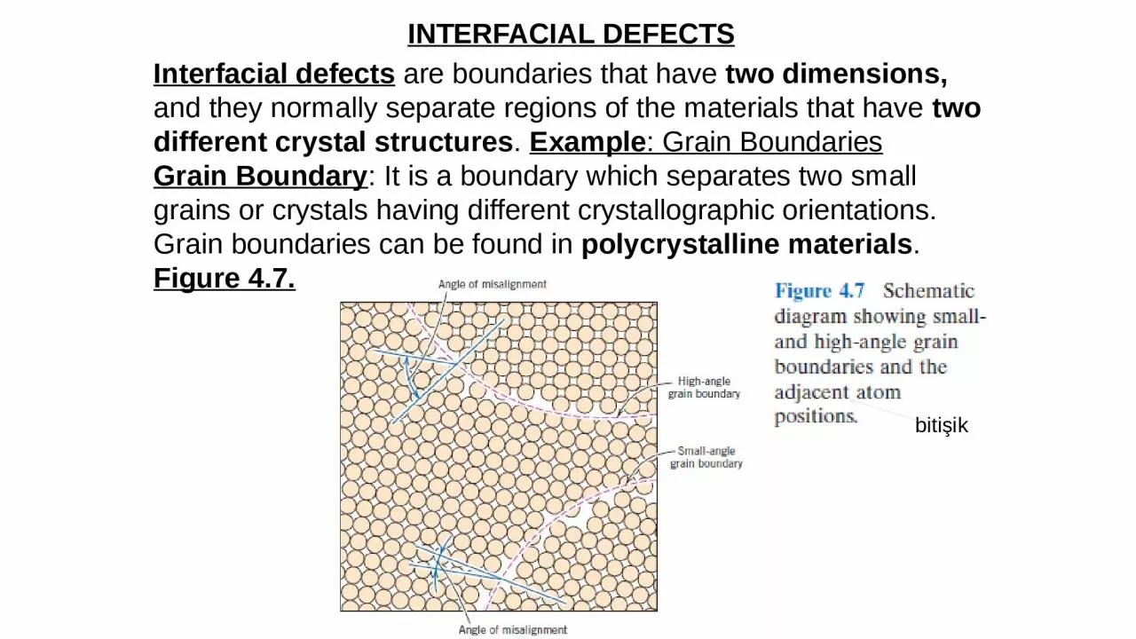
are boundaries that have two dimensions and they normally separate regions of the materials that have two different crystal structures Example Grain Boundaries Grain Boundary ID: 1046898

surface electron bonding microscope electron surface microscope bonding grain dimensions optical materials microscopy terms tem sample boundaries electrons crystal

Share:

Link:

Embed:

Download Presentation from below link

Download Presentation The PPT/PDF document "INTERFACIAL DEFECTS Interfacial defects" is the property of its rightful owner. Permission is granted to download and print the materials on this web site for personal, non-commercial use only, and to display it on your personal computer provided you do not modify the materials and that you retain all copyright notices contained in the materials. By downloading content from our website, you accept the terms of this agreement.


Presentation Transcript

1. INTERFACIAL DEFECTSInterfacial defects are boundaries that have two dimensions, and they normally separate regions of the materials that have two different crystal structures. Example: Grain Boundaries Grain Boundary: It is a boundary which separates two small grains or crystals having different crystallographic orientations. Grain boundaries can be found in polycrystalline materials. Figure 4.7. bitişik

2. MICROSCOPIC EXAMINATION Macroscopic dimensions: They are dimensions which can be observed with the unaided eye (çıplak göz). Example: Large grains on the aluminium garbage can have diameters on the order of centimeters. Microscopic dimensions: They are dimensions which are on the order of microns and can be observed with a microscope. Microstructure: It is a term which describes the microscopic grain size and shape.

3. MICROSCOPYBoth optical and electron microscopes are commonly used in microscopy. These microscopes are used in the investigation of microstructures in materials. Photomicrograph: It is a photograph on which the image is recorded. 1. Optical Microscopy: The visible light is used as the source. Optical microscopy is used to study the surface microstructure of materials. All metals, many ceramics and polymers can be studied. Normally, careful surface preparations are necessary in order to look at a material with an optical microscope.

4. MICROSCOPYExample: Polishing a metal surface and etching (aşındırma) the surface with a special chemical. The minimum dimension that can be seen with an optical microscope is about 1 micrometer (m) (1.0 × 10⁻⁶ meters).2. Electron Microscopy: The electrons are used as the source for electron microscopy. The electrons are focused on the sample and the image is formed with magnetic lenses. The minimum dimension that can be seen with an electron microscope is about 1 Angstrom (Å) (1.0 × 10⁻¹⁰ meters).

5. a. Transmission Electron Microscope (TEM): TEM image is formed by an electron beam that passes through the sample. The sample must be prepared as a thin film. Magnifications of 1,000,000 is possible in TEM. TEM is usually used in the study of grain boundaries and dislocations b. Scanning Electron Microscope (SEM): The source is electrons. The surface of a sample is scanned with an electron beam. It is used in the surface characterization of materials. Magnifications of  50,000 is possible in SEM

6. Fluorescent ScreenElectron TubeWith MagneticLenses Inside~2.5 m longNitrogen TankSample HolderComputerData ScreenPhotographicCameraBox

7. HOMEWORKWhat are the Primary Interatomic Bonds? What are the differences between Ionic Bonding, Covalent Bonding and metallic Bonding? In your answer, compare them in terms of three different properties. Draw the schematic representations of ionic bonding and metallic bonding. Label all the important terms on the figures.

8. HOMEWORK2. What are the definitions of the crystalline and amorphous material? What is the difference between the BCC and FCC crystal structure? Draw their crystal structures.

9. HOMEWORKWhat is the difference between a vacancy and a dislocation? In your answer, please write the differences in terms of two different properties. Draw the structure of a vacancy, and define the important terms on the figure.