/
High voltage drive to within 1.3 V of supply rails High voltage drive to within 1.3 V of supply rails

High voltage drive to within 1.3 V of supply rails - PDF document

giovanna-bartolotta
giovanna-bartolotta . @giovanna-bartolotta
Follow
388 views
Uploaded On 2016-05-25

High voltage drive to within 1.3 V of supply rails - PPT Presentation

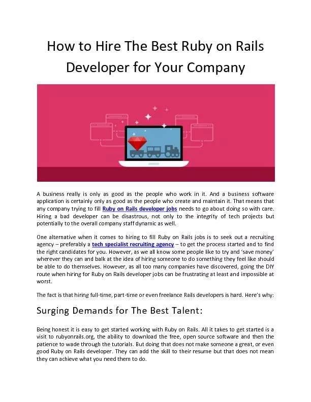
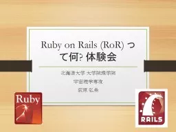
FEATURES Output shortcircuit protection High update rates Fast 100 Mss 10bit input data update rate Low static power dissipation 07 W Includes STBY function Voltagecontrolled video refer ID: 335219

FEATURES Output short-circuit protection High

Share:

Link:

Embed:

Download Presentation from below link

Download Pdf The PPT/PDF document "High voltage drive to within 1.3 V of su..." is the property of its rightful owner. Permission is granted to download and print the materials on this web site for personal, non-commercial use only, and to display it on your personal computer provided you do not modify the materials and that you retain all copyright notices contained in the materials. By downloading content from our website, you accept the terms of this agreement.


Presentation Transcript

FEATURES High voltage drive to within 1.3 V of supply rails Output short-circuit protection High update rates Fast, 100 Ms/s, 10-bit input data update rate Low static power dissipation: 0.7 W Includes STBY function Voltage-controlled video reference (brightness) and full-scale (contrast) output levels INV bit reverses polarity of video signal 3.3 V logic, 9 V to 18 V analog supplies High accuracy voltage outputs Laser trimming eliminates the need for adjustments Flexible logic STSQ/XFR allow parallel AD8383 operation at various resolutions Fast settling into capacitive loads 30 ns settling time to 0.25% into 150 pF load Slew rate 460 V/µs Available in 48-lead 7 mm Figure 1 PRODUCT DESCRIPTION The AD8383 provides a fast, 10-bit latched decimating digital input that drives six high voltage outputs. 10-bit input words are sequentially loaded into six separate, high speed, bipolar DACs. Flexible digital input format allows several AD8383s to be used in parallel for higher resolution displa The AD8383 dissipates 0.7 W nominal static power. The STBY pin reduces power to a minimum with fast recovery. The AD8383 is offered in a 48-lead, 7 mm × 7 mm × 0.85 mm LFCSP package and operates over the commercial temperature range of 0°C to 85°C. AD8383 Rev. 0 | Page 3 of 16 SPECIFICATIONS Table 1. @25°C, AVCC = 15.5 V, DVCC = 3.3 V, T MIN = 0°C, T MAX = 75°C, VFS = 5 V, VREFLO = V1 = V2 = 7 V, unless otherwise noted Parameter Conditions Min Typ Max Unit VIDEO DC PERFORMANCE 1 T MIN to T MAX , DAC Code 450 to 800 VDE …7.5 +7.5 mV VCME …3.5 +3.5 mV REFERENCE INPUTS V1, V2 Range 5 AVCC … 4 V V2 to V1 Range …0.25 V V1 Input Current +0.2 µA V2 Input Current …7.5 µA VREFHI Range VREFHI  VREFLO VREFLO AVCC V VREFLO Range VREFHI  VREFLO V1 … 0.5 AVCC … 1.3 V VREFHI Input Resistance To VREFLO 20 k VREFLO Bias Current …0.2 µA VREFHI Input Current 125 µA VFS Range 2 0 5.5 V RESOLUTION Coding Binary 10 Bits DIGITAL INPUT CHARACTERISTICS Maximum Input Data Update Rate 3 100 Ms/s CLK to Data Setup Time 0 ns CLK to STSQ Setup Time 1 ns CLK to XFR Setup Time 1 ns CLK to Data Hold Time 3 ns CLK to STSQ Hold Time 3 ns CLK to XFR Hold Time 3 ns CLK High Time 3 ns CLK Low Time 2.5 ns C IN 3 pF I IH 0.05 µA I IL 0.6 µA I IL , CLK 1.2 µA V IH 2 V V IL 0.8 V V TH 1.5 V VIDEO OUTPUT CHARACTERISTICS Output Voltage Swing AVCC … VOH, VOL … AGND 1.1 1.3 V CLK to VID Delay 4 50% of VIDx 10.0 12.0 14.0 ns INV to VID Delay 50% of VIDx 10.4 12.4 14.4 ns Output Current 100 mA Output Resistance 22  1 VDE = Differential Error Voltage = Common-Mode Error Voltage. See section. Theory of Operation 2 VFS = 2 × (VREFHI … VREFLO). 3 Maximum input transition time (10% to 90%) = 0.8/(2f) where f is the operating CLK rate. 4 Measured from 50% of falling CLK edge to 50% of output change. Measurement is made for both states of INV. AD8383 Rev. 0 | Page 5 of 16 ABSOLUTE MAXIMUM RATINGS Table 2. AD8383 Stress Ratings Parameter Rating Supply Voltages AVCCx … AGNDx 18 V DVCC … DGND 4.5 V Input Voltages Maximum Digital Input Voltages DVCC + 0.5 V Minimum Digital Input Voltages DGND … 0.5 V Maximum Analog Input Voltages AVCC + 0.5 V Minimum Analog Input Voltages AGND … 0.5 V Internal Power Dissipation 8 LFCSP Package @ 25°C Ambient 3.8 W Operating Temperature Range 0°C to 85°C Storage Temperature Range …65°C to +125°C Lead Temperature Range (Soldering 10 sec) 300°C Stresses above those listed under the Absolute Maximum Ratings may cause permanent damage to the device. This is a stress rating only; functional operation of the device at these or any other conditions above those indicated in the operational section of this specification is not implied. Exposure to the absolute maximum ratings for extended periods may reduce device reliability. 8 48-Lead LFCSP Package:  JA = 26°C/W (Still Air): JEDEC STD, 4-layer board with 0 CFM airflow  JC = 20°C/W  JB = 11.0°C/W in Still Air MAXIMUM POWER DISSIPATION Junction Temperature The maximum power that can be safely dissipated by the AD8383 is limited by its junction temperature. The maximum safe junction temperature for plastic encapsulated devices as determined by the glass transition temperature of the plastic is approximately 150°C. Exceeding this limit temporarily may cause a shift in the parametric performance due to a change in the stresses exerted on the die by the package. Exceeding a junction temperature of 175°C for an extended period can result in device failure. Overload Protection The AD8383 employs a 2-stage overload protection circuit that consists of an output current limiter and a thermal shutdown. The maximum current at any one output of the AD8383 is internally limited to 100 mA, average. In the event of a momen-tary short-circuit between a video output and a power supply rail (AVCC or AGND), the output current limit is sufficiently low to provide temporary protection. The thermal shutdown debiases the output amplifier when the junction temperature reaches the internally set trip point. In the event of an extended short-circuit between a video output and a power supply rail, the output amplifier current continues to switch between 0 mA and 100 mA typical with a period determined by the thermal time constant and the hysteresis of the thermal trip point. The thermal shutdown provides long-term protection by limiting the average junction temperature to a safe level. Operating Temperature Range Production testing guarantees a minimum thermal shutdown junction temperature (T J ) of at least 125°C. To ensure operation at T J ° it is necessary to limit the maximum power dissipation as described in the Applications section. Exposed Paddle The die paddle must be soldered to AVCC for reliable electrical operation. See the Applications section for details regarding use of the exposed paddles to dissipate excess heat. ESD CAUTION ESD (electrostatic discharge) sensitive device. Electrostatic charges as high as 4000 V readily accumulate on the human body and test equipment and can discharge without detection. Although this product features proprietary ESD protection circuitry, permanent damage may occur on devices subjected to high energy electrostatic discharges. Therefore, proper ESD precautions are recommended to avoid performance degradation or loss of functionality. AD8383 Rev. 0 | Page 6 of 16 PIN CONFIGURATION AND FU AD8383TOP VIEW7mm 7mm(Not to Scale)NC1DB02DB13DB24DB35VID0AVCC0,1VID13635 DB46DB57DB68DB79DB810AVCC2,3VID3313027 DB911VID526 NC12AGND525PIN 1INDICATOR DVCC AVCCBIASSTBYBYPAVCCDAC C VREFHIVREFLO NC23V238 Figure 2. 48-Lead LFCSP Pin Configuration Table 3. Pin Function Descriptions Pin Name Function Description DB(0:9) Data Input 10-Bit Data Input. MSB = DB(0:9). CLK Clock Clock Input. STSQ Start Sequence The state of STSQ is detected on the active edge of CLK. A new data loading sequence begins on the next active edge of CLK after STSQ is detected HIGH. The active CLK edge is the rising edge when E/O is held HIGH. It is the falling edge when E/O is R/L Right/Left Select A new data loading sequence begins on the left with Channel 0 when thisen this input is HIGH. E/O Even/Odd Select input is held HIGH and the falling edge when Data is loaded sequentially on the rising edges of CLK when this input is HIGH and on the falling edges when this input is LOW. XFR Data Transfer XFR is detected and a data transfer is initiated on a rising CLK edgeo outputs on the next rising CLK edge after XFR is detected. VID0…VID5 Analog Outputs These pins are directly connected to the an V1, V2 Reference Voltages The voltage applied between these pins set the reference levels of the analog outputs. Full-Scale References The voltage applied between ll-scale output voltage. When this pin is HIGH, the analog output voltages are above output voltages are below VMID. VMID is a hypothetical reference level set by the voltages applied to V1 and V2. VMID is equal to (V1 + V2)/2. DVCC Digital Power Supply Digital Power Supply. DGND Digital Supply Return This pin is normally AVCCx Analog Power Supplies Analog Power Supplies. AGNDx Analog Supply Returns Analog Supply Returns. BYP Bypass A 0.1 µF capacitor connected between this pin and AGND ensures optimum settling time. STBY Standby When HIGH, the internal AD8383 Rev. 0 | Page 8 of 16 THEORY OF OPERATION TRANSFER FUNCTION AND ANALOG OUTPUT VOLTAGE The DecDriver has two regions of operation: where the video output voltages are either above or below a reference voltage VMID, and where VMID = (V1 + V2)/2. The transfer function defines the analog output voltage as the function of the digital input code as follows: 1023…1)(nFSV … V1nVIDx for INV = LOW 1023…1)(nVFS2VnVIDx for INV = HIGH where n = input code VFS = 2 × (VREFHI … VREFLO) A number of internal limits define the usable range of the analog output voltages, VIDx, as shown in Figure 5. To best correlate transfer function errors to image artifacts, the overall accuracy of the DecDriver is defined by two parameters, VDE and VCME. VDE, the differential error voltage, measures the difference between the rms value of the output and the rms value of the ideal. The defining expression is VFSn1VnVOUTP2VnVOUTNnVDE102312)()()( VCME, the common-mode error voltage, measures ½ the dc bias of the output. The defining expression is 2…)()(2121)(2V1VnVOUTPnVOUTNnVCME INPUT CODEVIDx (V)AGNDV1–VFSV1V2VMIDV2+VFSAVCC0102304513-0-005 0VFS5.5V 0VFS5.5V 5VV2AVCC– 4)VMID = (V1+V2)/22VREFHI–VREFLO 5VV1AVCC– 4) 9VAVCC18V1.3V1.3VINV = HIGHINV = LOWINTERNAL LIMITS ANDUSABLE VOLTAGE RANGES Figure 5. Transfer Function, VIDx vs. Input Code, Internal Limits and Usable Output Voltage Range AD8383 Rev. 0 | Page 14 of 16 OUTLINE DIMENSIONS PIN 1INDICATOR TOPVIEW 6.75BSCSQ 7.00BSC SQ 148121337362425 BOTTOMVIEW 5.255.10 SQ4.95 0.500.400.30 0.300.230.18 0.50 BSC 12° MAX0.20REF0.80 MAX0.65 TYP 1.000.850.80 5.50REF 0.05 MAX0.02 NOM 0.60 MAX 0.60 MAX PIN 1INDICATOR COPLANARITY0.08SEATINGPLANE 0.25MIN COMPLIANT TO JEDEC STANDARDS MO-220-VKKD-2 Figure 16. 48-Lead Frame Chip Scale Package [LFCSP] (CP-48) Dimensions shown in millimeters ORDERING GUIDE Model Temperature Range Package Description Package Option AD8383ACPZ 9 0°C to 85°C 48-Lead LFCSP CP-48 9 Z = Pb-free part. AD8383 Rev. 0 | Page 15 of 16 NOTES AD8383 Rev. 0 | Page 16 of 16 © 2004 Analog Devices, Inc. All rights reserved. Trademarks and registered trademarks are the property of their respective owners. D03191…0…1/04(0) AD8383 Rev. 0 | Page 15 of 16 OBSOLETE AD8383 Rev. 0 | Page 16 of 16 © 2004 Analog Devices, Inc. All rights reserved. Trademarks and registered trademarks are the property of their respective owners. D03191…0…1/04(0) OBSOLETE AD8383 Rev. 0 | Page 14 of 16 PIN 1INDICATOR TOPVIEW BSCSQ 7.00BSC SQ 148121337362425 BOTTOMVIEW 5.255.10 SQ 0.50 0.300.230.18 0.50 BSC 0.20REF 1.00 5.50REF 0.05 MAX 0.60 MAX 0.60 MAX PIN 1INDICATOR COPLANARITY0.08SEATINGPLANE 0.25MIN Figure 16. 48-Lead Frame Chip Scale Package [LFCSP] (CP-48) Dimensions shown in millimeters Temperature Range Package Description AD8383ACPZ90°C to 85°C 48-Lead LFCSP CP-48 Z = Pb-free part. OBSOLETE AD8383 Rev. 0 | Page 13 of 16 PPPCPPCBPCBJCTCASETPCB AIR-CASETATJ04513-0-015 Figure 15. Simplified Thermal Equivalent Circuit Verification of the Maximum Operating Junction Temperature In order to verify the system thermal design for compliance with the maximum operating junction temperature specifica-tion, temperature measurements TCASE and T are required at the maximum possible total power dissipation in a complete, fully assembled LCD projection system. Maximum possible total power dissipation of the AD8383 occurs when the video input to the projector is a pattern with 1-pixel-wide white and black vertical lines. An alternative pattern that results in the maximum possible total power dissipation is a 1-pixel checkerboard pattern. The expected total power dissipation of the AD8383 in a 60 Hz, 6-channel XGA projector displaying the 1-pixel-wide vertical line or checker-board pattern is 1.08 W (at AVCC = 15.5 V, VCOM = 7 V, and LCD capacitance = 150 pF). Although the case and PCB temperatures are highly dependent on the PCB design, their measured values are expected to be similar at approximately 40°C above the ambient (on a typical PCB with a minimal airflow whose thermal design follows the recommendations described in this note). The junction temper-ature then calculates to approximately 10°C above the case and PCB temperatures. At a 70°C ambient temperature, the junction temperature is expected to be at approximately 120°C. The AD8383 has a relatively small thermal mass. In order to minimize measurement errors due to the thermal mass of the measuring device, a small-gauge thermocouple or a thermal probe with a very small thermal mass is required for the mea-surement of TCASE and TPower-Up and Power-Down Sequencing As indicated in the Absolute Maximum Ratings, the voltage at any input pin cannot exceed its supply voltage by more than 0.5 V. To ensure compliance with the Absolute Maximum Ratings, power-up and power-down sequencing may be required. During power-up, initial application of nonzero voltages to any of the input pins must be delayed until the supply voltage ramps up to at least the highest maximum operational input voltage. During power-down, the voltage at any input pin must reach zero during a period not exceeding the hold-up time of the power supply. Failure to comply with the Absolute Maximum Ratings may result in functional failure or damage to the internal ESD diodes. Damaged ESD diodes may cause temporary parametric failures, which may result in image artifacts. Damaged ESD diodes cannot provide full ESD protection, thus reducing reliability. The recommended sequence is Power ON Apply power to supplies. Apply power to other I/Os. Power OFF Remove power from I/Os. Remove power from supplies. In order to avoid image flicker, a bias voltage of approximately 1 V minimum must be maintained across the pixels of HTPS LCDs. The AD8383 provides two methods of maintaining this bias voltage. Internal Bias Voltage Generation Standard systems that internally generate the bias voltage reserve the upper-most code range for the bias voltage and use the remaining code range to encode the video for gamma correction. OBSOLETE AD8383 Rev. 0 | Page 5 of 16 ABSOLUTE MAXIMUM RATINGS Table 2. AD8383 Stress Ratings Supply Voltages AVCCx … AGNDx DVCC … DGND 4.5 V Input Voltages Maximum Digital Input Voltages DGND … 0.5 V Maximum Analog Input Voltages AVCC + 0.5 V AGND … 0.5 V Internal Power Dissipation LFCSP Package @ 25°C Ambient Operating Temperature Range 0°C to 85°C …65°C to +125°C Lead Temperature Range (Soldering 10 sec) 300°C Stresses above those listed under the Absolute Maximum Ratings may cause permanent damage to the device. This is a stress rating only; functional operation of the device at these or any other conditions above those indicated in the operational section of this specification is not implied. Exposure to the absolute maximum ratings for extended periods may reduce device reliability. 48-Lead LFCSP Package: = 26°C/W (Still Air): JEDEC STD, 4-layer board with 0 CFM airflow = 11.0°C/W in Still Air MAXIMUM POWER DISSIPATION Junction Temperature The maximum power that can be safely dissipated by the AD8383 is limited by its junction temperature. The maximum safe junction temperature for plastic encapsulated devices as determined by the glass transition temperature of the plastic is approximately 150°C. Exceeding this limit temporarily may cause a shift in the parametric performance due to a change in the stresses exerted on the die by the package. Exceeding a junction temperature of 175°C for an extended period can result in device failure. Overload Protection The AD8383 employs a 2-stage overload protection circuit that consists of an output current limiter and a thermal shutdown. The maximum current at any one output of the AD8383 is internally limited to 100 mA, average. In the event of a momen-tary short-circuit between a video output and a power supply rail (AVCC or AGND), the output current limit is sufficiently low to provide temporary protection. The thermal shutdown debiases the output amplifier when the junction temperature reaches the internally set trip point. In the event of an extended short-circuit between a video output and a power supply rail, the output amplifier current continues to switch between 0 mA and 100 mA typical with a period determined by the thermal time constant and the hysteresis of the thermal trip point. The thermal shutdown provides long-term protection by limiting the average junction temperature to a safe level. Operating Temperature Range Production testing guarantees a minimum thermal shutdown junction temperature (T) of at least 125°C. To ensure operation at T ° it is necessary to limit the maximum power dissipation as described in the Applications section. Exposed Paddle The die paddle must be soldered to AVCC for reliable electrical operation. See the Applications section for details regarding use of the exposed paddles to dissipate excess heat. Electrostatic charges as high as 4000 V readily accumulate on the human body and test equipment this product features proprietary ESD protection subjected to high energy electrostatic discharges. Therefore, proper ESD precautions are recommended to avoid performance degradation or loss of functionality. OBSOLETE AD8383 Rev. 0 | Page 10 of 16 PCB DESIGN FOR GOOD THERMAL PERFORMANCE The total maximum power dissipation of the AD8383 is partly dependent on load. In a 6-channel 60 Hz XGA system running at a 65 MHz clock rate, the total maximum power dissipation is 1.08 W at an LCD panel input capacitance of 150 pF. At the maximum specified clock rate of 100 Ms/s, the total maximum power dissipation can exceed 2 W for large capacitive loads, as shown in Table 4. Although the maximum safe operating junction temperature is higher, the AD8383 is 100% tested at a junction temperature of 125°C. Consequently, the maximum guaranteed operating junction temperature is 125°C. To limit the maximum junction temperature at or below the guaranteed maximum, the package, in conjunction with the PCB, must effectively conduct heat away from the junction. The AD8383s LFCSP package is designed to provide superior thermal characteristics, partly achieved by an exposed die paddle on the bottom surface of the package. In order to take full advantage of this feature, the exposed paddle must be in direct thermal contact with the PCB, which then serves as a heat sink. A thermally effective PCB must incorporate a thermal pad and a thermal via structure. The thermal pad provides a solderable contact surface on the top surface of the PCB. The thermal via structure provides a thermal path to the inner and bottom layers of the PCB to remove heat. THERMAL PAD DESIGN Thermal performance of the AD8383 varies logarithmically with the contact area between the exposed thermal paddle and the thermal pad on the top layer of the PCB. See Figure 11. (of the AD8383 mounted on a standard JEDEC PCB) is reduced by approximately 40% as the contact area increases from 0% (no thermal pad) to 50%. It approaches its specified value as the contact area (on the JEDEC standard PCB) approaches 100%. In order to minimize thermal performance degradation of production PCBs, the contact area between the thermal pad and the PCB should be maximized. Therefore, the size of the thermal pad should match the exposed 5.25 mm × 5.25 mm paddle size. However, if the PCB design rules require a pad-to-pad clearance of more than 0.3 mm, the size of the thermal pad may be reduced to 5 mm × 5 mm. Additionally, a second thermal pad of the same size should be placed on the bottom side of the PCB. At least one thermal pad should be in direct thermal (and electrical) contact with the AVCC plane. (°C/W) 250507510004513-0-011 Figure 11. Thermal Performance vs. Contact Area (on a JEDEC PCB) Table 4. Power Dissipation vs. Load Capacitance and VFS at 100 Ms/s Clock Rate VFS = 5 V VFS = 4 V QUIESCENTDYNAMICDYNAMIC 150 0.7 0.72 200 0.7 0.96 250 0.7 1.20 300 0.7 1.44 OBSOLETE AD8383 Rev. 0 | Page 9 of 16 APPLICATIONS The V1 and V2 inputs in these systems are tied together and are normally connected to VCOM, as shown in Figure 6. V2 V1 VCOM AD838304513-0-006 Figure 6. Standard Connection Diagram The transfer function of the AD8383 is shown in Figure 7 for V2 = V1 = VCOM. VBIAS = 1VVCOM VFS = 5V VFS = 5VRESERVEDCODERANGEVBIAS = 1V 04513-0-007 1023 820 Figure 7. Output Transfer Function for Standard Connection EXTERNAL VBIAS GENERATION In systems that require improved brightness resolution and higher accuracy, the V1 and V2 inputs, connected to external voltage references, provide the necessary VBIAS while allowing the full code range to be used for gamma correction. sets the white drive voltage while INV = LOW and sets the white drive voltage while INV = HIGH. and are defined as VCOMVBIASVCOM VBIASTo ensure a symmetrical ac driving voltage, the difference between and VCOM must be equal to the difference between VCOM and VCOMVCOM The circuit in Figure 8 ensures symmetry to within 1 mV with a minimum component count. Bypass capacitors are not shown for clarity. The transfer function and the input symmetry error of the AD8383 are shown in Figure 9 when the circuit of Figure 8 is used to generate VBIAS. AVCC = 15.5V VZ = 5.1V DVCC = 3.3V V COM = 7VR1 = 6kR2 = 1kV2 = 8VV1 = 6V V2 V1 AD8383AD8132 6 3218V–V+VCOM–IN+IN54 04513-0-008 Figure 8. High Accuracy Reference Circuit VBIAS = 1VVCOMV2V1 VFS = 4V VFS = 4VVBIAS = 1V A SYMMETRICAL OUTPUT AT 85°C WHENITS SUPPLY, (V+)– (V–), IS AT 7.2V. 1023 Figure 9. Transfer Function for High Accuracy Reference Applications 5.76.26.77.27.78.28.79.29.710.210.7–8.75–6.25–3.75–1.25–7.50–5.00–2.50(V2 + V1)/2– VCOM (mV) TA = 85°C TA = 25°C TYPICAL ASYMMETRY AT THE OUTPUTS OF THEAD8383 VERSUS ITS POWER SUPPLY FOR THE04513-0-010 Figure 10. Accuracy for High Accuracy Reference Applications OBSOLETE AD8383 Rev. 0 | Page 8 of 16 THEORY OF OPERATION TRANSFER FUNCTION AND ANALOG OUTPUT VOLTAGE The DecDriver has two regions of operation: where the video output voltages are either above or below a reference voltage VMID, and where VMID = (V1 + V2)/2. The transfer function defines the analog output voltage as the function of the digital input code as follows: ×=…1)(FSV … V1nVIDx for INV = LOW ×=…1)(VFS2VnVIDx for INV = HIGH where = input code VREFLOA number of internal limits define the usable range of the analog output voltages, VIDx, as shown in Figure 5. To best correlate transfer function errors to image artifacts, the overall accuracy of the DecDriver is defined by two parameters, VDE and VCME. VDE, the differential error voltage, measures the difference between the rms value of the output and the rms value of the ideal. The defining expression is n1VnVOUTP2VnVOUTNnVDE−−−−)()()(VCME, the common-mode error voltage, measures ½ the dc bias of the output. The defining expression is …)()()(2V1VnVOUTPnVOUTNnVCME VIDx (V)V1–VV2+V 0VFS5.5V 0VFS5.5V AVCC– 4) AVCC– 4) 9VAVCC18V1.3V1.3VINV = HIGHINV = LOWINTERNAL LIMITS ANDUSABLE VOLTAGE RANGES Figure 5. Transfer Function, VIDx vs. Input Code, Internal Limits and Usable Output Voltage Range OBSOLETE AD8383 Rev. 0 | Page 7 of 16 CLKDB(0:9)STSQXFR04513-0-003VTH = 1.65VVTH = 1.65VVTH = 1.65VVTH = 1.65VtCLK LOWtCLK HIGHtHOLDtSKEWtSETUPtSETUPtHOLD Figure 3. Timing Diagram, Even Mode (E/O = HIGH) Figure 4. Timing Diagram, Odd Mode (E/O = LOW) OBSOLETE AD8383 Rev. 0 | Page 6 of 16 PIN CONFIGURATION AND FU AD8383TOP VIEW7mm 7mm(Not to Scale)NC1DB02DB13DB24DB35VID0AVCC0,1VID13635 DB46DB57DB68DB79DB810AVCC2,3VID3313027 DB911VID526 NC12AGND525PIN 1INDICATOR DVCC AVCCBIASSTBYBYPAVCCDAC C VREFHIVREFLO NC23V238 Figure 2. 48-Lead LFCSP Pin Configuration Table 3. Pin Function Descriptions Pin Name Function DB(0:9) Data Input ta Input. MSB = DB(0:9). CLK Clock Clock Input. STSQ Start Sequence The state of STSQ is detected on the active edge of CLK. A new data loading sequence begins on the next active edge of CLK after STSQ is detected HIGH. The active CLK edge is the rising edge when E/O is held HIGH. It is the falling edge when E/O is R/L Right/Left Select A new data loading sequence begins on the left with Channel 0 when thisen this input is HIGH. E/O Even/Odd Select input is held HIGH and the falling edge when Data is loaded sequentially on the rising edges of CLK when this input is HIGH and on the falling edges when this input is LOW. XFR Data Transfer XFR is detected and a data transfer is initiated on a rising CLK edgeo outputs on the next rising CLK edge after XFR is detected. VID0…VID5 Analog Outputs These pins are directly connected to the an V1, V2 Reference Voltages The voltage applied between these pins set the reference levels of the analog outputs. Full-Scale References The voltage applied between ll-scale output voltage. When this pin is HIGH, the analog output voltages are above output voltages are below VMID. VMID is a hypothetical reference level set by the voltages applied to V1 and V2. VMID is equal to (V1 + V2)/2. DVCC Digital Power Supply Digital Power Supply. DGND Digital Supply Return This pin is normally AVCCx Analog Power Supplies Analog Power Supplies. AGNDx Analog Supply Returns Analog Supply Returns. BYP Bypass A 0.1 µF capacitor connected between this pin and AGND ensures optimum settling time. STBY Standby OBSOLETE AD8383 Rev. 0 | Page 4 of 16 Parameter Conditions Min SPECIFICATIONS (continued) VIDEO OUTPUT DYNAMIC PERFORMANCE C, MIN Data Switching Slew Rate 20% to 80% 460 V/µs Invert Switching Slew Rate ime to 1% ime to 0.25% Invert Switching Settling Time to 1% Invert Switching Settling Time to 0.25% Invert Switching Overshoot CLK and Data Feedthrough5 10 mV p-p All-Hostile Crosstalk Amplitude 40 mV p-p Duration 20 ns DAC Transition Glitch Energy Code 511 to Code 512 0.3 nV-s POWER SUPPLY DVCC, Operating Range 3 3.3 3.6 V DVCC, Quiescent Current 20 28 mA AVCC, Operating Range 9 18 V Total AVCC Quiescent Current STBY AVCC Current STBY = H STBY DVCC Current STBY = H OPERATING TEMPERATURE RANGE, T AMBIENT TEMPERATURE RANGE OPERATING TEMPERATURE RANGE, T Measured on two outputs differentially as CLK and DB(0:9) are driven and STSQ and XFR are held low. Measured on two outputs differentially as the other four outputs make a full-scale transition for both states of INV. Operation at 85°C ambient temperature requires a thermally optimized PCB layout (see Application Notes), minimum airflow of 200 lfm, input clock rate not ack-to-white transition 4 V, C OBSOLETE AD8383 Rev. 0 | Page 3 of 16 SPECIFICATIONS Table 1. @25°C, AVCC = 15.5 V, DVCC = 3.3 V, T = 0°C, T = 75°C, VFS = 5 V, VREFLO = V1 = V2 = 7 V, unless otherwise noted VIDEO DC PERFORMANCEMIN, DAC Code 450 to 800 VDE …7.5 +7.5 mV VCME …3.5 +3.5 mV REFERENCE INPUTS V1, V2 Range 5 AVCC … 4 V V2 to V1 Range V1 Input Current V2 Input Current VREFHI Range VREFHI  VREFLO VREFHI  VREFLO VREFHI Input Resistance VREFLO Bias Current …0.2 µA VREFHI Input Current 125 µA VFS Range2 5.5 V RESOLUTION Coding 10 Bits DIGITAL INPUT CHARACTERISTICS Maximum Input Data Update Rate CLK to Data Setup Time CLK to STSQ Setup Time 1 ns CLK to XFR Setup Time CLK to Data Hold Time 3 ns CLK to STSQ Hold Time 3 ns CLK to XFR Hold Time CLK High Time 3 ns CLK Low Time 2.5 ns CIN 3 pF IIH 0.05 µA IIL 0.6 µA IIL, CLK 1.2 µA VIH V VIL 0.8 V VTH 1.5 V VIDEO OUTPUT CHARACTERISTICS Output Voltage Swing AVCC … VOH, VOL … AGND CLK to VID Delay450% of VIDx 10.0 12.0 14.0 ns INV to VID Delay 50% of VIDx 10.4 12.4 14.4 ns Output Current 100 mA Output Resistance 22  VDE = Differential Error Voltage = Common-Mode Error Voltage. See section. Theory of Operation VFS = 2 × (VREFHI … VREFLO). Maximum input transition time (10% to 90%) = 0.8/(2f) where f is the operating CLK rate. Measured from 50% of falling CLK edge to 50% of output change. Measurement is made for both states of INV. OBSOLETE AD8383 Rev. 0 | Page 2 of 16 TABLE OF CONTENTS Specifications.....................................................................................3Absolute Maximum Ratings............................................................5Maximum Power Dissipation.....................................................5Pin Configuration and Function Descriptions.............................6Timing Diagrams..............................................................................7Theory of Operation........................................................................8Transfer Function and Analog Output Voltage........................8Applications.......................................................................................9External VBIAS Generation........................................................9PCB Design for Good Thermal Performance........................10Thermal Pad Design..................................................................10Thermal Via Structure Design..................................................11Solder Masking...........................................................................11Reference PCB Design...............................................................11Estimated Junction Temperature.............................................12Outline Dimensions.......................................................................14Ordering Guide..........................................................................14Revision 0: Initial Version OBSOLETE Low Cost 10-Bit, 6-Channel OutputDecimating LCD DecDriver® AD8383 Information furnished by Analog Devices is believed to be accurate and reliable. However, no responsibility is assumed by Analog Devices for its use, nor for any infringements of patents or other rights of third parties that may result from its use. Specifications subject to change without notice. No license is granted by implication or otherwise under any patent or patent rights of Analog Devices. Trademarks and registered trademarks are the property of their respective owners.One Technology Way, P.O. Box 9106,Tel: 781.329.4700Fax: 781.326.8703© 2004 Analog Devices, Inc. All rights reserved. High voltage drive to within 1.3 V of supply rails High update rates Fast, 100 Ms/s, 10-bit input data update rate Low static power dissipation: 0.7 W Includes STBY function Voltage-controlled video reference (brightness) and full-scale (contrast) output levels INV bit reverses polarity of video signal 3.3 V logic, 9 V to 18 V analog supplies High accuracy voltage outputs Laser trimming eliminates the need for adjustments STSQ/XFR allow parallel AD8383 operation at various Fast settling into capacitive loads 30 ns settling time to 0.25% into 150 pF load Slew rate 460 V/µs Available in 48-lead 7 mm × 7 mm LFCSP package APPLICATIONS LCD analog column driver FUNCTIONAL BLOCK DIAGRAM INVV1V2Figure 1PRODUCT DESCRIPTION The AD8383 provides a fast, 10-bit latched decimating digital input that drives six high voltage outputs. 10-bit input words are sequentially loaded into six separate, high speed, bipolar DACs. Flexible digital input format allows several AD8383s to be used in parallel for higher resolution displays. STSQ synchronizes sequential input loading, XFR controls synchronous output updating, and R/L controls the direction of loading as either left-to-right or right-to-left. Six channels of high voltage output drivers drive to within 1.3 V of the rail. For maximum flexibility, the output signal can be adjusted for dc reference, signal inversion. The AD8383 is fabricated on the 26 V, fast bipolar XFHV process developed by Analog Devices, Inc. This process provides fast input logic, bipolar DACs with trimmed accuracy and fast settling, high voltage, precision drive amplifiers on the same chip. The AD8383 dissipates 0.7 W nominal static power. The STBY pin reduces power to a minimum with fast recovery. The AD8383 is offered in a 48-lead, 7 mm × 7 mm × 0.85 mm LFCSP package and operates over the commercial temperature range of 0°C to 85°C. OBSOLETE AD8383 Rev. 0 | Page 12 of 16 AD8383PCBCPCBPCBTPCBJCJC-BOTTOMCJC-BOTTOMTJCAIR-PCBAIR-PCBCAIR-CASEAIR-CASETATAMBIENTCJCTCASECP, JB,JB04513-0-014 Figure 14. Thermal Equivalent Circuit ESTIMATED JUNCTION TEMPERATURE Assuming no heat flows through the sides of the AD8383 pack-age, heat flow from the AD8383 is through two paths. While part of the total heat generated dissipates through the top of the case, the remainder flows into the PCB to be dissipated. Assuming there is no other heat-generating component near the AD8383, the thermal equivalent circuit of a system that consists of one AD8383 mounted on a PCB is shown in Figure 14. The thermal resistance of the top of the case, , is constant, independent of the system variables, and well defined. depends on the thermal resistance of the molding compound. The thermal resistance of the system, , is system dependent and therefore cannot be properly estimated. Although it is tra-ditional to provide the thermal resistance of a JEDEC reference system in the data sheet, its value may not be appropriate for all systems and may result in large erro��rs (25%). The thermal resistance of production PCBs, , depends largely on the particular PCB design, and, to some extent, the environ-mental conditions specific to the particular system. Although is traditionally not provided on data sheets, a thermal character-ization parameter, , of a JEDEC reference system is gaining increasing acceptance. When the PCB thermal design near the AD8383 closely approximates the PCB of the JEDEC reference system,  approaches For thermally enhanced packages, the thermal resistance of the exposed thermal paddle, JC-BOTTOM, is very low and may therefore be ignored. Junction Temperature and Maximum Power Dissipation In a thermal steady state represented by the simplified schema-tic shown in Figure 15, heat flow from the die is partly through the top of the case, causing a temperature drop (CASE), and partly through the PCB, causing a temperature drop (). The junction temperature is calculated as follows: CBPPCBJTTTTPPP)()(== PCBJCPCBJCPCBJC T T  P where: is the junction temperature CASE is the temperature of the top of the case (near the output pins for the AD8383) is the PCB temperature on the solder side (directly under the AD8383) is the total power dissipated by the AD8383 is the thermal resistance of the top of the case is the thermal resistance of the PCB At a given maximum allowed junction temperature, the maximum allowed power dissipation is −−PCBJCPCBJC For a thermally optimized PCB, can be replaced with and the equation can be rewritten as −−PCBJC  OBSOLETE AD8383 Rev. 0 | Page 11 of 16 THERMAL VIA STRUCTURE DESIGN Effective heat transfer from the top to the inner and bottom layers of the PCB requires thermal vias incorporated into the thermal pad design. Thermal performance increases logarithmi-cally with the number of vias, as shown in Figure 12. With the AD8383 on a standard JEDEC PCB,  reaches its specified value when a total of 16 vias are used. At a via count above 36, approaches its optimum value as the slope of the curve approaches zero. (°C/W) 100203004513-0-01240 Figure 12. Thermal Performance vs. Number of Vias (on a JEDEC PCB) Near optimum thermal performance of production PCBs is attained when the number of vias is at least 36. To minimize the formation of solder voids due to solder flowing into the via holes (solder wicking), the via diameter should be small. Solder masking of the via holes on the top layer of the PCB plugs the via holes, inhibiting solder flow into the holes. To optimize the thermal pad coverage, the solder mask diameter should be no more than 0.1 mm larger than the via diameter. The top copper layer is shown in Figure 13. 7 mm 7 mm Figure 13. Recommended PCB Landing The bottom thermal pad forms AVCC plane. Thermal PadsTop PCB Layer: 5.25 mm × 5.25 mm Bottom PCB Layer: 5.25 mm × 5.25 mm Thermal via structure Diameter: 0.25 Number of vias: 41 Via Grid Pitch: 0.5 mm MiscellaneousPerimeter Pads: 0.5 mm × 0.25 mm Solder Mask Swell: 0.02 mm OBSOLETE