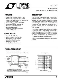
/
Designing High-Voltage, Programmable Power Supply for driving High-current Designing High-Voltage, Programmable Power Supply for driving High-current

Designing High-Voltage, Programmable Power Supply for driving High-current - PowerPoint Presentation

kittie-lecroy
kittie-lecroy . @kittie-lecroy
Follow
360 views
Uploaded On 2018-11-09

Designing High-Voltage, Programmable Power Supply for driving High-current - PPT Presentation

P ulsed loads Part 3 Presented by Sanjay Pithadia SEM Industrial Systems Medical Sector Challenge to Solve Scaling Voltage and Current using standard voltage regulators and MOSFETs 2 Voltage Scaling to support Higher Input Voltage ID: 724373

voltage current mosfet scaling current voltage scaling mosfet high regulator input mosfets regulators www tida tool vin driver http

Share:

Link:

Embed:

Download Presentation from below link

Download Presentation The PPT/PDF document "Designing High-Voltage, Programmable Pow..." is the property of its rightful owner. Permission is granted to download and print the materials on this web site for personal, non-commercial use only, and to display it on your personal computer provided you do not modify the materials and that you retain all copyright notices contained in the materials. By downloading content from our website, you accept the terms of this agreement.


Presentation Transcript

Slide1

Designing High-Voltage, Programmable Power Supply for driving High-current Pulsed loadsPart - 3

Presented by: Sanjay Pithadia

SEM – Industrial Systems, Medical SectorSlide2

Challenge to SolveScaling Voltage and Current using standard voltage regulators and MOSFETs

2Slide3

Voltage Scaling – to support Higher Input Voltage


The regulator’s operating input voltage range decides VIN and VG values

Truly scalable

Can be increased by adding more BJTs

VIN = Input Voltage

VG = Virtual Ground Voltage

To Input of Voltage Regulator

3Slide4

High Output Current Regulators

Linear and Switching Voltage Regulator

Fundamental (App Note)

http://

www.ti.com/lit/an/snva558/snva558.pdf

Limited by Die size, package and thermal transfer

4Slide5

High-Current Low-Noise Parallel LDO Reference

Design

http://

www.ti.com/tool/TIDA-01232

Safe Operating Curve

Size and Cost

Current Scaling – Parallel Regulators

5Slide6

Current Scaling – Paralleling MOSFETs (Positive Regulator)

Current Sensing

Low-impedance MOSFET Driver

6

 Slide7

Current Sensing

Low-impedance MOSFET Driver

Current Scaling – Paralleling MOSFETs (Negative Regulator)

7

 Slide8

Ballast Resistors – to take care of V

GS

effects

All drains are connected together

All sources are connected together

MOSFET V

GS

Drop across 0.47

Ω

Total V

GS

required to turn-on MOSFET

8

V

GS

= 3V

V

GS

= 4VSlide9

Selecting MOSFET for Scaling Current


CSD19533KCS


9Slide10

TIDA-01371 is available on TI.com10

Visit

www.ti.com/tool/TIDA-01371

to find design resources (Gerbers, Schematics and more).Slide11

TI Information – Selective Disclosure