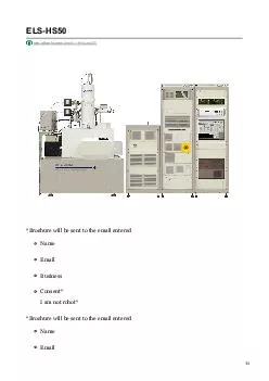
PPT-Ion Beam Lithography: Focused Ion Beam & Ion Projection Lithography

Author : kittie-lecroy | Published Date : 2018-10-21

Ziam Ghaznavi CHE 384T Lithography November 30 th 2017 1 OutlineAgenda Motivation Ion Solid Interactions Overview of IBL Systems Future Outlook 2 Motivation SEMATECH

Presentation Embed Code

Download Presentation

Download Presentation The PPT/PDF document "Ion Beam Lithography: Focused Ion Beam ..." is the property of its rightful owner. Permission is granted to download and print the materials on this website for personal, non-commercial use only, and to display it on your personal computer provided you do not modify the materials and that you retain all copyright notices contained in the materials. By downloading content from our website, you accept the terms of this agreement.

Ion Beam Lithography: Focused Ion Beam & Ion Projection Lithography: Transcript


Ziam Ghaznavi CHE 384T Lithography November 30 th 2017 1 OutlineAgenda Motivation Ion Solid Interactions Overview of IBL Systems Future Outlook 2 Motivation SEMATECH and the ITRS. Michael Johnston. 4/13/2015. Abstract and Outline. Nanoscale Lithography. . is an ever growing fabrication process due to technology demands. We are continuously striving to increase the number of transistors on a chip to increase performance. The drive for smaller and faster technologies has caused the development of fabrication techniques that allow us to work at the nanoscale feature size. A few lithography techniques will be explored to show how this whole process works. The processes I will cover include Photo, Electron Beam and X-Ray lithography. These forms of lithography share a common process of preparation exposure and development while fabricating wafers.. NANO 101. Introduction to Nanotechnology. 1. 2. Lithography. Photolithography. Electron beam lithography. X-ray lithography. Focused ion beam lithography. “Photoengraving”. Transfer pattern into reactive polymer film (“resist”). . kjetil. Lithography is the process of transferring patterns. Photolithography. Positive resist. Negative resist. X-ray lithography. E-beam lithography. Photolithography. General process: . Cleaning of wafer. EE 4611 . Dehua . liu. 4/8/2016. THE origin of Nanoscale Lithography. Major methods . of Nanoscale . Lithography. A. dvantages and disadvantages of different methods of Nanoscale . Lithography. Moore’s . EE 4611 . Dehua . liu. 4/8/2016. THE origin of Nanoscale Lithography. Major methods . of Nanoscale . Lithography. A. dvantages and disadvantages of different methods of Nanoscale . Lithography. Moore’s . Ziam Ghaznavi. CHE 384T Lithography. November 30. th. , 2017. 1. Outline/Agenda. Motivation. Ion – Solid Interactions. Overview of IBL Systems . Future Outlook. 2. Motivation. SEMATECH and the ITRS. Ion source and optics.. Ion-solid interaction, damage.. Scanning ion beam imaging.. FIB lithography using resist.. FIB milling, sputtering yield.. Redeposition.. Single line milling.. Other types of FIB lithographies (implantation, intermixing…).. Introduction.. Photon-based lithography: DUV (deep UV), EUV (extreme UV), X-ray. Charged-beam based lithography: electron beam, focused ion beam. Nanofabrication by molding/printing: soft lithography, nanoimprint. Electron Beam Lithography System - ELF 10000 Electron Beam Lithography System HS50 University of Illinois Urbana-Champaign to Install First 150kV Electron Beam Lithography System in North America Harvard’s Center for Nanoscale Systems(CNS) will install North America’s first High Speed Elionix ELS-HS50 electron beam lithography system. This will be the third Elionix electron beam lithography system installed into the Harvard CNS cleanroom. Nanoscale fabrication techniques have taken device, systems and material design to a new level. Electron Beam Lithography (EBL) enables the creation of highly accurate nanoscale structures. Solid state physics. . Lecture (8). Nanolithography. Introduction. Nanolithography is a growing field of techniques within nanotechnology dealing with the engineering (etching, writing, printing) of nanometer-scale structures. From Greek, the word can be broken up into three parts: ".

Download Document

Here is the link to download the presentation.
"Ion Beam Lithography: Focused Ion Beam & Ion Projection Lithography"The content belongs to its owner. You may download and print it for personal use, without modification, and keep all copyright notices. By downloading, you agree to these terms.

Related Documents