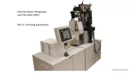
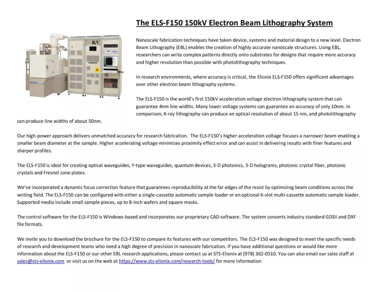
/
The ELS-F150 150kV Electron Beam Lithography System The ELS-F150 150kV Electron Beam Lithography System

The ELS-F150 150kV Electron Beam Lithography System - PDF document

stselionix
stselionix . @stselionix
Follow
357 views
Uploaded On 2021-07-18

The ELS-F150 150kV Electron Beam Lithography System - PPT Presentation

Nanoscale fabrication techniques have taken device systems and material design to a new level Electron Beam Lithography EBL enables the creation of highly accurate nanoscale structures ID: 856125

Electron Beam Lithography

Share:

Link:

Embed:

Download Presentation from below link

Download Pdf The PPT/PDF document "The ELS-F150 150kV Electron Beam Lithogr..." is the property of its rightful owner. Permission is granted to download and print the materials on this web site for personal, non-commercial use only, and to display it on your personal computer provided you do not modify the materials and that you retain all copyright notices contained in the materials. By downloading content from our website, you accept the terms of this agreement.


Presentation Transcript

The ELS - F150 150kV Electron Beam Lithography System Nanoscale fabrication techniques have taken device, systems and material design to a new level. Electron Beam Lithography (EBL) enables the creation of highly accurate nanoscale structures. Using EBL, researchers can write complex patterns directly onto substrates for designs that require more accuracy and higher resolution than possible with photolithography techniques. In research environments, where accuracy is critical, the Elionix ELS - F150 offers significant advantages over other electron beam lithography systems. The ELS - F150 is the world’s first 150kV acceleration voltage electron lithography system that can guarantee 4nm line widths. Many lower voltage systems can guaran tee an accuracy of only 10nm. In comparison, X - ray lithography can produce an optical resolution of about 15 nm, and photolithography can produce line widths of about 50nm. Our high - power approach delivers unmatched accuracy for research fabrication. The ELS - F150’s higher acceleration voltage focuses a narrower beam enabling a smaller beam diameter at the sample. Higher accelerating voltage minimizes proximity effect error and can assist in deliverin g results with finer features and sharper profiles. The ELS - F150 is ideal for creating optical waveguides, Y - type waveguides, quantum devices, 3 - D photonics, 3 - D holograms, photonic crystal fiber, photonic crystals and Fresnel zone plates. We’ve incorporated a dynamic focus correction feature that guarantees reproducibility at the far edges of the resist by optimizing beam conditions across the writing field. The ELS - F150 can be configured with either a single - cassette automatic sample loader or an optional 6 - slot multi - cassette automatic sample loader. Suppor ted media include small sample pieces, up to 8 - inch wafers and square masks. The control software for the ELS - F150 is Windows - based and incorporates our proprietary CAD software. The system converts industry standard GDSII and DXF file formats. We invi te you to download the brochure for the ELS - F150 to compare its features with our competitors. The ELS - F150 was designed to meet the specific needs of research and development teams who need a high degree of precision in nanoscale fabrication. If you have additional questions or would like more information about the ELS - F150 or our other EBL research applications, please contact us at STS - Elionix at (978) 362 - 0510. You can also email our sales staff at sales@sts - elionix.com or visit us on the web at https://www.sts - elionix.com/research - tools/ for more information View & Download Original Source @ https://www.sts - elionix.com/the - els - f150 - 150kv - electron - beam - lithography - system/