PPT-Electron-beam lithography
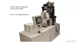
with the Raith EBPG Part 2 Choosing parameters M Rooks Yale University Choosing ebeam exposure parameters Step 1 choose the resist and choose the resist thickness
Download Presentation
"Electron-beam lithography" is the property of its rightful owner. Permission is granted to download and print materials on this website for personal, non-commercial use only, provided you retain all copyright notices. By downloading content from our website, you accept the terms of this agreement.
Presentation Transcript
Transcript not available.