/
Electron-beam lithography Electron-beam lithography

Electron-beam lithography - PowerPoint Presentation

tatiana-dople
tatiana-dople . @tatiana-dople
Follow
385 views
Uploaded On 2018-03-10

Electron-beam lithography - PPT Presentation

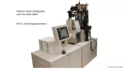
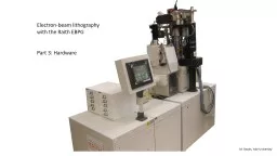
with the Raith EBPG Part 3 Hardware M Rooks Yale University EBPG 5000 System Hardware 100 kV accelerating potential electrons of course 20 bit main field DAC Digital to Analog Converter ID: 646222

substrate beam piece field beam substrate field piece stage laser focus ebpg exposure height pattern wafer spot sample work

Share:

Link:

Embed:

Download Presentation from below link

Download Presentation The PPT/PDF document "Electron-beam lithography" is the property of its rightful owner. Permission is granted to download and print the materials on this web site for personal, non-commercial use only, and to display it on your personal computer provided you do not modify the materials and that you retain all copyright notices contained in the materials. By downloading content from our website, you accept the terms of this agreement.


Presentation Transcript

Slide1

Electron-beam lithography

with the Raith EBPGPart 3: Hardware

M. Rooks, Yale UniversitySlide2

EBPG 5000+ System Hardware

100 kV accelerating potential electrons of course20 bit main field DAC Digital to Analog Converter*14 bit trapezium DAC for filling shapes50 MHz maximum clock minimum dwell time 1/50 ms6 inch stage 15 cm for you communists

Two-stage magnetic deflection

* You should know the meaning of “DAC” and “LSB”. Look it up.Slide3

Electron Source

At the top of the column is the electron source, a thermal field emitter. Electrons are drawn out of the sharp tungsten tip by an extraction potential around 2 kV.The emitter pin is kept hot so that ZrO will flow down the surface, thereby lowering the work function and producing a larger current. Keeping the tip hot also makes the source more stable.

This is exactly the same type of electron source commonly found in SEMs and TEMs.

(Older systems used hot LaB

6

emitters, but we do not speak of that.)Slide4

Electron Optics

Electrons are generated from a field emitter in the gun, then focused by an electrostatic lens (C1) before accelerating through the anode.The magnetic lens (C2) focuses the beam to a crossover in the blanking cell, which is simply a plate which can be charged up to turn the beam off. Placing this blanking plate at the crossover allows the beam to turn off without shifting the image.

The third lens (C3) is the objective, focusing the electrons to a spot on the sample. Inside C3 is a smaller, faster coil for rapid tweaks to the focus. The beam is automatically refocused every time the sample moves.

Just like a SEM, the column contains coils to correct astigmatism, also adjusted automatically.Slide5

Stage Control

The position of the stage is measured with a laser interferometer, with an accuracy below one nanometer. The interferometer uses a He-Ne laser and Zeeman splitting to create a GHz range beat frequency at the receivers. This frequency shifts as the stage moves, and so the Doppler effect can be used to measure the stage speed.

S

peed is integrated to find the stage position.

Motors on the stage move in a sloppy manner, while the laser signal is used to deflect the beam electronically, thereby compensating for any jerky mechanical motion or mechanical vibration.Slide6

Main Field

Deflecton ErrorsThe EBPG uses the laser stage to automatically calibrate and compensate for gain, rotation, keystone and pincushion errors.Additionally, the focus and stigmation are dynamically corrected over the deflection field.

If you ever wonder why the big system is better than a converted SEM, this is the answer.

X, Y gain errors

X, Y axis rotation errors

Field keystone errors

Pincusion

and third-order distortionSlide7

Stigmation

coils &

fast focus

More

sigmation

&

fast focus coils

Secondary electron detectors – four unbiased scintillators on light pipes, with photomultipliers

Electron Optics – Bottom

Directly above the sample stage are the fast focus and

stigmation

coils.

Secondary electrons from the sample (usually a silicon wafer) are detected by four scintillators on the ends of light-pipes, coupled to photomultiplier tubes. These detectors are similar to those in SEMs, but without the usual 300V bias drawing in the electrons. A bias on the ends of the detectors would distort the writing field. Unfortunately, without the bias these detectors are not very efficient.

Other e-beam systems detect secondary electrons using a diode mounted under the objective lens, or with a scintillator built into the objective lens. It would be nice to have these more efficient detectors, but you can’t have everything.Slide8

Laser projects spot onto surface of substrate.

Substrate

Signals from Dual-diode detector

determines distance moved

by laser beam.

Laser spot movement due to change in height of substrate surface.

System reads change in spot position on Dual Diode detector

Laser spot reflected onto detector.

Reflected laser beam

Laser Height Sensor

Every time the stage moves, a height sensor corrects the focus and deflection gain.

If the laser beam hits the wafer’s edge or hits a metal fixture, then the height reading will fail. For this reason,

patterns should be placed at least 1mm from any edge

– especially if you are using a fixture for a small substrate.Slide9

As the substrate height varies, the system must correct both focus and field size.

Correcting the field size is critical, since this determines field stitching accuracy. You can see now why smaller field block sizes lead to smaller stitching errors.

On

the EBPG you should keep the block size less than 700

m

m

so that field stitching errors will be less than 50 nm. The maximum block size is equal to the maximum field, 1 mm. But it would be a mistake to use such a large deflection.

Substrate Height CorrectionSlide10

Substrate Surface

Focal Plain

Objective lens & aperture

Spot defocused and

astigmatic

when deflected

Beam focused to form round spot at Field

center

.

Errors caused by beam deflection

When the beam is deflected, the EBPG system corrects the focus, astigmatism, and field size. Dynamic focus, astigmatism, field gain, and height adjustment are all calibrated automatically before each exposure.Slide11

Exposure Strategy

The slower 20-bit main deflector positions the beam in the field, then the fast 14-bit trapezium deflector fills in each shape.

Software breaks a pattern into exposure fields (“blocks”) so that a large pattern can be stitched together by moving the stage.

Inside each field the shapes are broken into simple parallelograms.

Inside each parallelogram the beam paints the shape with a serpentine raster.Slide12

EBPG Sample Holders

Top left: holder for 5 inch mask plates. Top right: wafer holder. Bottom left: two two-inch wafers (we do not have this one). Bottom right: piece holder. This is a bottom-reference piece holder which we do not have at Yale. This holder requires manual trimming to level the substrate and to move it into the correct plane. The next slide shows a better design

.

At Yale we have holders for 3, 4, and 6 inch wafers, as well as adapters for smaller substrates.Slide13

sample

Adapters For Small Pieces

These fixtures fit in place of a 4 inch wafer. The small substrate will be at the proper focus height, determined by its top surface. This is a better design than the one on the previous slide, because any junk on the back of the substrate will not tilt the sample, nor move it out of the focus plane.

These fixtures are built at Yale, and so it is easy to make holders customized for your weird samples. Currently, we have fixtures with window sizes of 8mm, 10mm, 20mm, 38mm, and 2 inch (50mm). Your substrate must have one dimension at least 2mm larger than the window size.Slide14

Substrate fixturing

ideas that do not workFile under “It seemed like a good idea at the time” these bad ideas:Gluing the piece to a big wafer with PMMA, photoresist, or glue. Terrible idea – the solvent will not completely dry under the piece. In the vacuum system the solvent will boil, and the piece will pop off.

Using vacuum grease to hold the piece. This is less stupid, but you will have a hard time getting the grease off the substrate, and you cannot put vacuum grease in the developer.

Building an adapter with a “V” shaped window. Sorry – the angle will always be wrong, and the adapter will cover alignment marks, etc.

Building an adapter with adjustable top rails. This idea is too complicated and too easily broken. We’ve been there, done that, and it doesn’t work.Slide15

Substrate fixturing

ideas that sometimes workClipping the wafer to a metal puck. This does work sometimes, but it requires a lot of fussing. The puck has to be shimmed to the correct plane, and the back of the wafer must be cleaned to avoid tilting. If the clip pushes down on a delicate spot, the substrate can easily break.

Taping the substrate to a large wafer, with carbon tape. This does work, but the previous comments about shimming and cleaning also apply. In addition to fussing with shims, you will get carbon tape goo on the substrate. Also there is a risk of breaking the piece when removing the carbon tape.

Using

crystalbond

wax to attach the little piece to a wafer. Yes, we have done this with diamonds, but it’s tricky. The substrate is not grounded, and so it must be coated with gold (on top of the resist). The wax can go into IPA/water or TMAH developer, and it can later be removed in acetone. The wafer/wax/diamond can go from the e-beam to developer, and then to the evaporator or etcher. The tricky bit is that liftoff in acetone will also lift off the little piece.

Raith’s

own butt-end clips (seen a few slides back) also work, after a fashion. Unfortunately, brittle materials like GaAs and

InP

tend to break when pushed from the side. You’ll also have the fun of trimming the height.Slide16

Small Substrates Are BadUsing substrates smaller than 1 cm is

stupid for a number of reasons:Resist edge beak ruins the exposure within 1mm of the edge.Piece-part fixtures will cover another 2mm of the

stubstrate

.

The laser height sensor will not operate closer than 1mm to the window, which means that you will lose 4 mm in one dimension and 2 mm in the other. That’s quite a lot off lost real estate on a 10mm piece.

Alignment of a multi-layer device will be very difficult, because the piece must be pre-aligned to within 0.2 degrees. That means your alignment marks must be on-axis within 35

m

m over 10mm. That’s not fun at all.

If you are trying to save money by chopping up an expensive substrate, then think about how much e-beam time you are wasting by misaligning the substrate. One hour of

ebeam

time is $100. How much did you save?

It takes 6 minutes to vent and 6 minutes to pump the load lock, as well as ~ 10 minutes to find your alignment marks. Therefore each piece has an overhead cost around $37. How much did you really save by chopping up a $50 wafer? Do the math.Slide17

Running the EBPG – preparing a pattern

Start by designing a pattern, then convert it to EBPG format with the program Beamer.Use cjob to set up the exposure, specifying the exposure dose and pattern placement on the substrate.Finally, coat the substrate with resist, put it in the EBPG, and start the exposure.

CAD

e.g. with “layout”

O

utput GDS format

pattern conversion with “beamer”

Output GPF format

exposure setup

with “

cjob

Output job

script

pattern check

with “cview”

exposure on EBPG

with “beams” Slide18

Running the EBPG – a simple exposure

Cjob produces a script that runs your exposure, but this is not required. You could expose a pattern with a simple set of commands, as shown here. Just type them into a terminal window.Complex jobs use the same commands, with more elaborate scripts created by cjob.

pg

info arc beam

list beam files (that contain lens settings)

pg

arc restore beam 10na_300um_2

set the lenses for 10nA beam current

mcur

measure the beam current

pg

select pattern

abc.gpf choose a pattern

pg

set resist 800.0

set the dose

pg

adjust

ebpg

calibration

pg

move position 75mm,75mm

move somewhere

pg expose pattern

expose! Slide19

End of part 3

Now you should proceed to the quiz.