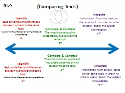
Describe the differences between positive and negative photoresist Explain why photolithography requires a clean environment Classify cleanrooms using both ISO and US FED standards Describe the process of a ID: 701877
Download Presentation The PPT/PDF document "Photolithography Identify the basic step..." is the property of its rightful owner. Permission is granted to download and print the materials on this web site for personal, non-commercial use only, and to display it on your personal computer provided you do not modify the materials and that you retain all copyright notices contained in the materials. By downloading content from our website, you accept the terms of this agreement.
Slide1
Photolithography
Identify the basic steps of a photolithographic process
Describe the differences between
positive
and
negative
photoresist
Explain why photolithography requires a clean environment
Classify
cleanrooms
using both ISO and US FED standards
Describe the process of a
RCA clean
Describe the process of applying resist via
spinning
and calculate the resulting resist thicknesses
Describe, compare and contrast the exposure processes of
Contact printing
Proximity printing
Projection printing
Calculate the
resolutions
of the above processes and explain what they depend on and why
Define and calculate
depth of focus
and explain how it is related to resolution in projection printing
Define the terms
Dose
and
dose to clear
,
Light intensity
,
Resist sensitivity
, and
Contrast
Calculate sensitivity and contrast for both positive and negative resist
Explain the shape of
resist profiles
and calculate the slopes of resist layer
Explain the need for and use of
alignment marks
Explain how
photo masks
are
producedSlide2
Reminder of the photolithography steps in the μ-machining process
Silicon wafer
SiO
2
Spin on photoresist
Glass plate
Opaque region
Unexposed photoresist removed by developer
Mask
Exposed
photoresist
becomes less
soluableSlide3
Reminder of the photolithography steps in the μ-machining process
Note the pattern is the opposite of that on the mask. This is true for
negative
photoresist.Slide4
Keeping it clean
Photolithography
can be the “bottle neck” in terms of how small you can make a MEMS structure.
Dust particles on masks behave as extra opaque regions (
lugares
oscuros) and transfer unwanted patterns. Photolithography must be done is a very clean environment.Slide5
Clean rooms
Clean rooms
are classified based on how many particles of a certain six exist within a certain volume:
In
the
EE. UU.Class 1
less than 1 particle > 0.5 μm/ft3Class 10 less than 10 particles > 0.5 μm/ft3Class 100
less than 100 particles > 0.5 μm/ft3Class 1000 less than 1000 particles > 0.5 μm/ft3
Outside the US (ISO 14644-1)ISO Class 1 less than 10 particles > 0.1 μm/m3ISO Class
2 less than 100 particles > 0.1 μm/m3ISO Class 3 less than 1000 particles > 0.1 μm/m3Slide6
Comparison of cleanroom standards
Slide7
Comparison of cleanroom standards
Equivalency of cleanroom classifications
C
n
= 10
N (0.1 / D)2.08ISO 14644-1US FED STD 209E
ISO 1-ISO 2-ISO 3Class 1ISO 4Class 10ISO 5Class 100ISO 6Class 1000ISO 7Class 10,000
ISO = log(US) + 3US
= 10(ISO - 3)Slide8
Clean room etiquette and requirements
“
Bunny suits
”
required (main source of airborne dust is human skin)Not constructed near sources of pollutionFloors are conductive for electrostatic
discharge.Only certain types furniture are allowedSpecially designed paper (pens no pencils)No eating and drinkingPerfume, cologne and makeup are
discouraged.Rose-Hulman students in the clean room facility at RHIT¿Por qué parece tan amalliro
?Slide9
Wafer cleaning
RCA clean
Developed
by
Werner Kern
in 1965 while working at RCA Laboratories1:1:5 to 1:1:7 by volume solution of NH4OH : H
2O2 : H2O is used to remove organic contaminants and heavy metalsHCl : H2O2 : H2O in a 1:1:5 to 1:2:8 volume ratio is used to remove aluminum, magnesium, and light alkali
ionsBoth steps approximately 20 minutes while gently heating to 75-85°C on a hot plateThere are other cleaning techniques, such as “piranha clean”Slide10
Photoresist
Often called “resist”
Three (3) components
:
a
base resin, which is a polymer: gives the resist structure
photoactive compound (PAC): The light-sensitive componentsolvent.Comes in two varietiesPositive resistNegative resist
Photoresist is the “stuff” of photolithographyUsually sensitive to a narrow band of ultraviolet (UV) lightSlide11
Positive versus negative resist
Positive
resist
Exposure
degrades the PAC
Becomes
more soluble to the developer after exposureUnexposed regions of the resist are left behind after developmentDeveloped resist pattern is identical to the mask pattern. Alkalis such as NaOH or KOH used as developers
Very sensitive to UV light with wavelength of 365 nm, called the I-line of the mercury spectrumNegative resist Exposure increases MW of resist or creates new insoluble products
Becomes less soluble to the developer after exposureUnexposed regions of the resist are removed after developmentDeveloped resist pattern is the opposite of the mask pattern. Organic solvents such as benzene used as developersVery sensitive to UV light with wavelength of 405
nm, called the H-line of the mercury spectrum~ 10 times more sensitive than positive resistSlide12
Positive versus negative resist
Slide13
Te
toca
a ti
The mask shown in the figure is used to transfer a pattern to a silicon wafer. Sketch the resulting pattern on the wafer after exposure and development for both positive and negative resist.. Also sketch the profile from the side of the wafer.
Positive resist
Negative resist
Mask
Side view of waferSlide14
Applying resist
Pour it onto wafer
Spin wafer to
distribute the solution across
surface
Photoresist
can also be sprayed (which may or may not get around uniformity issues)
Three steps
A
pre-bake to reduce water (water can
the reduce adhesion of resist)Spin on the resistA post-bake to remove the solventSlide15
Applying resist
T
is the film
thickness
C
is polymer concentration,η is viscosity, ω is rotational spin speed, and
K, α, β, and γ are experimentally determined constants that vary from system to system.
Coating step (proceso de cubrirlo) poses the largest danger from a dust contamination.
An empirical relation often used to predict the film thickness is given by
Spinning creates a slight vacuum along the plane of the wafer entraining airborne dust particlesSlide16
Te
toca
a ti
With a given spinner and photoresist formulation, a spin speed
of 4000
rpm gives a resist thickness of 0.7μm. How would you create a resist layer
a. 0.8 μm thick?b. 1.0 μm?Slide17
Exposure and pattern transfer
Two
basic
types of machinesContact
aligner from University of Alabama Center for Materials for Information Technology
Projection “stepper” from Cornell NanoScale Science and Technology Facility¿Por qué parece tan
amalliro?Projection printerContact alignerSlide18
Ultraviolet light spectrum
Ultraviolet light
regions
Emission
spectrum for an Hg-
Xe lamp
Photoresist made to be sensitive to ultraviolet (UV) light.Hg-Xe lamps often used as light source.Slide19
Contact and proximity printing
Contact printing
Proximity printing
Contact printing and proximity printing create features in the photoresist that more or less look just like the mask.Slide20
Projection printing
In projection printing the size of the features on the resist can be different that on the mask itself.
A generic lithographic projection systemSlide21
Projection printing
Photolithography
is
an optical
printing process
f
f
s
s'Slide22
Te
toca
a ti
A projection printing system is to reduce the size of mask features by a facture of 5. If the objective lens is kept 60 mm from the surface of the wafer, what should the focal length of the objective be?
f
f
s
s'
Respuesta
: 50 mmSlide23
Dose, dose to clear, and
arial
image
latent image
Dose
to clear
Dose required
to expose
the resist
so that it completely
develops
D
p
for positive
resist (completely develops away)
D
g
0
for negative resist (completely remains)
D
Dose
Optical energy
per
unit surface
area
D
=
It
exposure
I
Light intensity
Optical power
per
unit surface
area
[W/m
2
]Slide24
Development and post-treatment
Positive
resist
Exposure degrades the PAC
Becomes
more soluble
to the developer after exposureUnexposed regions of the resist are left behind after developmentDeveloped resist pattern is identical to the mask pattern. Alkalis such as NaOH or KOH used as developers
Negative resist Exposure increases MW of resist or creates new insoluble productsBecomes less soluble to the developer after exposureUnexposed regions of the resist are removed after developmentDeveloped
resist pattern is the opposite of the mask pattern. Organic solvents such as benzene used as developers
DeveloperSlide25
Development and post-treatment
After exposure, a mild oxygen
plasma
can be used to remove leftover exposed/unexposed resist.
A
post-bake follows, hardening resist even more.After the resist has done what it needs to do (act as a mask for doping, or for the etching of the layer below, e.g., ) resist needs to be removed completely
strippingPositive resist Wet stripping usually usedChemical solvent such as acetone
or methylethylketone (C4H8O)Often requires T ~ 80°CCan ignite with O2
!Safety importantNegative resist Harder to removeUse of acids and/or chlorinated hydrocarbons; e.g., H2SO4
and H2O2 at 150°C (“piranha” clean)Sometimes a plasma ash required.
Plasma ashingSlide26
Resolution
Diffraction
in contact and proximity printing
https://webspace.utexas.edu/cokerwr/www/index.html/double_slit.gif
http://www.colorado.edu/physics/phys2020/phys2020_sum98/lab_manual/Lab5/Image2088.gif
http://www.colorado.edu/physics/phys2020/phys2020_sum98/lab_manual/Lab5/Image2091.gif
Constructive dsin(θ)
= Destructive dsin(θ) =
m·λ(m + ½ λ)Slide27
Resolution
Resolution
: smallest
distinguishable feature size of a
transferred pattern
position
intensity
Contact and proximity printing
zSlide28
Resolution
Projection printing
Want a wide lens
close to the image
planeSlide29
Resolution
Relationship of numerical aperture to other quantities
Numerical aperture
NA
=
n
sin(θmax) = D/
2F where F = f/D (effective f number)
0.16 < NA < 0.60.3 < k1
< 1.1Slide30
Resolution
Contact/proximity
◄ How
do you increase resolution
? ►
ProjectionMake s small (s0 is contact printing short mask life)Make resist layer thin
Too thin and will not serve as good ion implantation mask, etc.develop awayMake λ smallMake numerical aperture bigBig lenses and costly optics
Other trade-offsMake λ smallSlide31
Resolution
Ultraviolet light
regions
Emission
spectrum for an Hg-
Xe lamp
¡Eso es la razón que usamos luz ultravioleta! smaller wavelengths better resolutionSlide32
Resolution—Depth of focus
Depth of focus: the distance across which the
aerial image
is in focus.
resist
δ
aerial image
δSlide33
Resolution—Depth of focus
structural or sacrificial layer
resist
δ
Variations in
the height of surface features
must be less than the
depth of focus
.
For the best results surfaces should be planar
(flat).Slide34
Sensitivity and resist profiles
Positive resist
Negative resist
sidewalls not verticalSlide35
Sensitivity and resist profiles
Positive resist
0
50
100
Resist remaining (%)
dose,
D
(
mJ
/cm
2
)
10
D
p
100
D
p
0
(+)
Dp
Dose to clearLithographic sensitivity
ContrastHigh γp sharp images (más
claro)Slide36
Sensitivity and resist profiles
Negative resist
0
50
100
Resist remaining (%)
dose,
D
(
mJ
/cm
2
)
10
D
gx
20
Dg
0Dg
i
For negative resist
dose to clear ≠ sensitivitysensitivity = Dg
xSlide37
Modeling of resist profiles
For positive resist:
λ
, wavelength
a
and
α are related to resist absorbanceDp, dose to cleark
2, process dependent contrast (same as in δ)k, depends on coherence of lightTo get vertical sidewalls:
Small wavelengthSmall absorbanceSmall dose to clearSmall k2 (small δ)Large NASlide38
Mask
alignment
Mask alignment also called registration
alignment mark
alignment mark
Processed wafer
Mask
Good to use asymmetry with alignment marks
Arrows (
flechas
) are
often used to make alignment marks easier to findSlide39
Mask types
Phase shift masks are used to enhance resolution
Binary mask
Phase shift mask
Alternating phase shift
Attenuating phase shift
Make thicker or thinner
Make less transparentSlide40
Mask materials
glass
High resolution emulsion (gelatin)
or
Thin (
l000-2000 Å
) metal, usually Cr Emulsion is photosensitive. Mask produced by photolithography
Glass first coated with metal. Photoresist coated on top and patterned.Metal etched through photoresist mask and resist is stripped.Slide41
Creating masks
Typically both processes use a
projection printing
machine called a
stepper
.