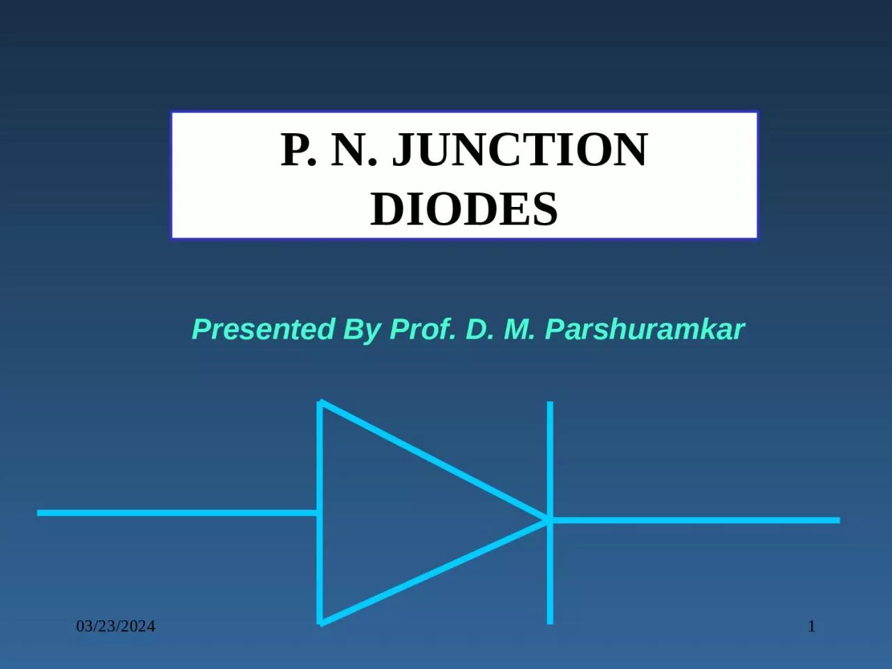
PPT-01/04/2018 1 P. N. JUNCTION DIODES
Author : layla | Published Date : 2023-11-11
Presented By Prof D M Parshuramkar NType Material NType Material When extra valence electrons are introduced into a material such as silicon an ntype material is
Presentation Embed Code
Download Presentation
Download Presentation The PPT/PDF document "01/04/2018 1 P. N. JUNCTION DIODES" is the property of its rightful owner. Permission is granted to download and print the materials on this website for personal, non-commercial use only, and to display it on your personal computer provided you do not modify the materials and that you retain all copyright notices contained in the materials. By downloading content from our website, you accept the terms of this agreement.
01/04/2018 1 P. N. JUNCTION DIODES: Transcript
Presented By Prof D M Parshuramkar NType Material NType Material When extra valence electrons are introduced into a material such as silicon an ntype material is produced The extra valence electrons are introduced by putting impurities or . Course . Code : . 11-EC201. DEPARTMENT . OF . ELECTRONICS & COMPUTER . ENGINEERING. The . two modes of operation of ideal diodes and the use of an external circuit to limit the forward current (a) and the reverse voltage (b).. Semester 1 . Lecturer: Javier . Sebastián. . Electrical Energy Conversion and Power Systems . Universidad. de Oviedo. Power Supply Systems. Review of the physical principles of operation of semiconductor devices.. Lecture. 3. 1. Discrete Semiconductor Devices. Semiconductor Materials. Conductor and Insulators.. N-type, P-Type, electron, and hole current. PN junction, depletion region, potential barrier.. Diodes. Aditya . Kuroodi. 2016. Relevant Course(s): EE121B, EE115A. Introduction to Transistors. Transistors: BJTs & MOSFETs. There are 2 main types of transistors: Bi-Polar Junction Transistors and Metal-Oxide Semiconductor Field Effect Transistor. Independent . Electronical. Stroboscope . LYS ELECTRONIQUE. 14 avenue du Général de Gaulle. 92360 MEUDON LA FORET. France. http://www.lys-electronique.com. info@lys-electronique.com. The . device. LEDEL ISRAEL LIGHTING LTD. 0522-741576. 32 W . Power . consumption. 3520 . Luminous. flux. OSRAM. Duris. E5 . diodes. IP66. Protection . level. 100 000 hours. lifetime. 5 years. guarantee. Usage. LED luminary L-line developed for agricultural facilities lighting, especially for bird-farms. Main distinction from general LED luminaries is strong resistance for aggressive environments and fluids used for farms treatments and high power consumption efficiency.. Cody Nascene. Jake Clifton. The semiconductor power diode has been used extensively in various power applications such as power rectifiers and power supplies. Diodes. Since the invention of semiconductor materials and the eventually birth of the modern day power diode, its usefulness has become apparent to engineers and other electrical designers. As new technology is improving efficiencies and versatility, engineers are finding more ways to use the power diode than ever before.. Bill Leonard N0CU. 7 April 2018. Topics. What damages receiver front ends. Common types of receiver front end protectors. Example: homebrew protector. What Damages Receiver Front Ends?. Damage results from exceeding a semiconductor’s junction breakdown voltage. Logan J Lauder. Background . 6.5 million E.Vs on the road today. Typically operating between 12V – 400V. DC or AC current . Overview . IGBTs for inverters and motor controllers. Fast switching power MOSFETS . PRODUCT CHANGE NOTICE FINAL UPDATENotification Date Implementation Date Product Family Change Type PCN August 17 2020 Discrete Additional Wafer Source / Assembly and Test Site / 2477 TITLE Additi Assistant Professor. Department of Electronics. St. Joseph’s College, . Trichy. . . What Are Diodes Made Out Of?. Silicon (Si) and Germanium (Ge) are the two most common single elements that are used to make Diodes. A compound that is commonly used is Gallium Arsenide (GaAs), especially in the case of LEDs because of it’s large bandgap. . Mobility is a measure of the ability of an electron or a hole to get around inside a semiconductor. Scattering events lower mobility. As the temperature of a semiconductor increases, there will be more and more lattice vibrations.. Wisam. J. Aziz. Solid state physics. . Lecture (4). A . p-n junction is an interface or a boundary between two semiconductor material types, namely the p-type and the n-type, inside a semiconductor.. Zero Biased Junction Diode. When . a diode is connected in a . Zero Bias. condition, no external potential energy is applied to the PN junction. However, if the diodes terminals are shorted together, a few holes (majority carriers) in the P-type material with enough energy to overcome the potential barrier will move across the junction against this barrier potential. This is known as the .
Download Document
Here is the link to download the presentation.
"01/04/2018 1 P. N. JUNCTION DIODES"The content belongs to its owner. You may download and print it for personal use, without modification, and keep all copyright notices. By downloading, you agree to these terms.
Related Documents