/
CACTI-IO: CACTI With CACTI-IO: CACTI With

CACTI-IO: CACTI With - PowerPoint Presentation

liane-varnes
liane-varnes . @liane-varnes
Follow
343 views
Uploaded On 2019-11-25

CACTI-IO: CACTI With - PPT Presentation

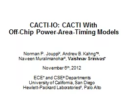
CACTIIO CACTI With OffChip PowerAreaTiming Models Norman P Jouppi Andrew B Kahng Naveen Muralimanohar Vaishnav Srinivas November 6 th 2012 ECE and CSE Departments ID: 768082

power chip bandwidth memory chip power memory bandwidth timing subsystem case capacity performance significant cacti area bus models boom

Share:

Link:

Embed:

Download Presentation from below link

Download Presentation The PPT/PDF document "CACTI-IO: CACTI With" is the property of its rightful owner. Permission is granted to download and print the materials on this web site for personal, non-commercial use only, and to display it on your personal computer provided you do not modify the materials and that you retain all copyright notices contained in the materials. By downloading content from our website, you accept the terms of this agreement.


Presentation Transcript

CACTI-IO: CACTI With Off-Chip Power-Area-Timing Models Norman P. Jouppi ¥ , Andrew B. Kahng †‡ , Naveen Muralimanohar ¥ , Vaishnav Srinivas † November 6 th , 2012 ECE † and CSE ‡ Departments University of California, San Diego Hewlett-Packard Laboratories ¥ , Palo Alto

AgendaIntroductionNeed for off-chip power-area-timing modelsCACTI-IO modelsCase studies using CACTI-IO: High-capacity DDR3 configurations 3-D stacking LPDDRx for servers Summary

Memory Subsystem Performance Latency/Access times: The Memory Wall Modern architectures try to hide the latency impact Capacity: Need for large server main memory Bandwidth: The Memory Bandwidth Limit Latency hiding techniques do not help Off-chip limits bandwidth Source: Rogers et al.Scaling the Bandwidth Wall: Challenges in and Avenues for CMP Scaling

Memory Subsystem PowerMemory subsystem power a significant portion

Memory Subsystem PowerMemory subsystem power a significant portionDRAM

Memory Subsystem PowerMemory subsystem power a significant portionDRAM, Buffers

Memory Subsystem PowerMemory subsystem power a significant portionDRAM, Buffers, Caches

Memory Subsystem PowerMemory subsystem power a significant portionDRAM, Buffers, Caches, Interconnect/IO/PHY

Memory Subsystem PowerMemory subsystem power a significant portionDRAM, Buffers, Caches, Interconnect/IO/PHYOff-chip IO power is a key component Source: Economou et al. Full-System Power Analysis and Modeling for Server Environments

Off-chip Performance Memory bandwidth limited by off-chip interface

Off-chip Performance Memory bandwidth limited by off-chip interface Source-synchronous signaling

Off-chip Performance Memory bandwidth limited by off-chip interface Source-synchronous signaling Signal/Power Integrity

Off-chip Performance Memory bandwidth limited by off-chip interface Source-synchronous signaling Signal/Power Integrity: ISI

Off-chip Performance Memory bandwidth limited by off-chip interface Source-synchronous signaling Signal/Power Integrity: ISI, Crosstalk

Off-chip Performance Memory bandwidth limited by off-chip interface Source-synchronous signaling Signal/Power Integrity: ISI, Crosstalk, Supply Noise

Off-chip Performance Memory bandwidth limited by off-chip interface Source-synchronous signaling Signal, power integrity: ISI, Crosstalk, Supply Noise Pincount

Off-chip PowerOff-chip power significant portion of the memory subsystem

Off-chip PowerOff-chip power significant portion of the memory subsystemHigher off-chip capacitance and voltages

Off-chip PowerOff-chip power significant portion of the memory subsystemHigher off-chip capacitance and voltagesTerminations and Vref -biased receivers

Off-chip PowerOff-chip power significant portion of the memory subsystemHigher off-chip capacitance and voltagesTerminations and Vref -biased receivers Clocking elements

Off-chip PAT Models For ArchitectsOff-chip models for full-system simulatorSimulators today do not account for IO/PHY powerAccurate off-chip power and performance numbers Co-optimize off-chip & on-chip power/performance Explore new off-chip topologies and technologies

CACTI-IOCACTI well known for memory architectsCACTI-IO includes off-chip PAT modelsCACTI-IO config file includes off-chip parameters CACTI-IO Tech Report available # Memory State (R=Read, W=Write, I=Idle or S=Sleep) //- iostate "R" -iostate "W"//-iostate "I"//-iostate "S"# Is ECC Enabled (Y=Yes, N=No)-dram_ecc "N"#Address bus timing //- addr_timing 0.5 //DDR, for LPDDR2 and LPDDR3 - addr_timing 1.0 //SDR for DDR3, Wide-IO //- addr_timing 2.0 //2T timing // addr_timing 3.0 // 3T timing # Bandwidth ( Gbytes per second, this is the effective bandwidth) - bus_bw 12.8 GBps # Memory Density ( Gbit per memory/DRAM die) - mem_density 2 Gb # IO frequency (MHz) (frequency of the external memory interface). - bus_freq 800 MHz # Duty Cycle (fraction of time in the Memory State defined above) - duty_cycle 1.0 # Activity factor for Data (0->1 transitions) per cycle (for DDR, need to account for the higher activity in this parameter. E.g. max. activity factor for DDR is 1.0, for SDR is 0.5) - activity_dq 1.0 # Activity factor for Control/Address (0->1 transitions) per cycle (for DDR, need to account for the higher activity in this parameter. E.g. max. activity factor for DDR is 1.0, for SDR is 0.5) - activity_ca 0 # Number of DQ pins - num_dq 1 # Number of DQS pins - num_dqs 0 //8 differential pairs # Number of CA pins - num_ca 0 # Number of CLK pins - num_clk 2 //1 differential pair # Number of Physical Ranks - num_mem_dq 2 //Number of ranks (loads on DQ and DQS) per DIMM or buffer chip # Width of the Memory Data Bus - mem_data_width 1 //x4 or x8 or x16 or x32 memories

AgendaIntroductionNeed for off-chip power-area-timing modelsCACTI-IO Models Case Studies using CACTI-IO: High-capacity DDR3 configurations 3-D Stacking BOOM: LPDDRx for serversSummary

Dynamic PowerDynamic Power (switching lumped caps) Interconnect Power t L  V SW  V dd / Z 0 if 2t L  t b t b  V SW  Vdd / Z0 if 2tL > t b

Termination PowerDQ:Multi rankFew termination types READ and WRITE Assume 50% 0’s, 1’s Includes Rx, Tx CA:Fly-by VDD/2 termination

PHY PowerReference generatorsVref-biased receiversClock distributionDLL/PLLPhase Rotators

Performance: Eye Compliance Timing Budget: Tx, Channel, and Rx (setup/hold) Voltage Budget: Tx (V OL /V OH ), Channel, Rx (VIL/VIH)

Channel JitterDOE for topology parametersRon/R tt / C dram some of the key parameters Linear interpolation of Taguchi array

Timing Budget

Voltage Budget

Area Driver area depends on R ON and R TT Predriver stages fanout to driver Fixed area for ESD and controls

ValidationCACTI-IO models account for off-chip power, area and timingValidation against SPICE Within 15% error across all the simulations Lookup tables validated by construction

Power for LPDDR2 DQ Single-Lane Total IO Power

Power for DDR3 DQ Single-Lane Termination Power Total IO Power

AgendaIntroductionNeed for off-chip power-area-timing modelsCACTI-IO Models Case Studies using CACTI-IO: High-capacity DDR3 configurations 3-D Stacking BOOM: LPDDRx for servers Summary

Case Studies Using CACTI-IOWe present three case studies:High-capacity DDR3 configurations3-D configurations BOOM (Buffered Output On Module): LPDDRx for servers Compare the configurations for: CapacityBandwidth IO Power EfficiencyBOOM case study with IO+DRAM power

Case Study 1: High-capacity DDR3RDIMM

Case Study 1: High-capacity DDR3RDIMM, LRDIMM

Case Study 1: High-capacity DDR3RDIMM, LRDIMM, BoB (Buffer on Board) BoB uses serial bus to host

Case Study 1: High-capacity DDR3 RDIMM, LRDIMM, BoB (Buffer on Board) BoB uses serial bus to host LRDIMM offers highest capacityBoB offers best bandwidth and power efficiency per GB of capacity

Case Study 2: 3-D StackingTSS basedPeak bandwidth of 176 GB/s for Micron’s Hybrid Memory Cube (HMC) Power efficiency varies by around 2X Source: Micron

BOOM: LPDDRx for serversBOOM (Buffered Output On Module) architecture from Hewlett-Packard:Buffer chip on the boardLPDDRx memories (lower speed, power) Wider bus from the buffer to the DRAMs Achieves better power efficiency using LPDDRx memories Still meets performance using buffer

BOOM Topology

Case Study 3: BOOM50% increase in IO efficiency with LPDDRxNo terminations with wider, slower buses Serial bus from the buffer offers more savings

BOOM: IO+DRAM Power

BOOM: IO+DRAM PowerIO power a significant portion of the combined power (DRAM+IO): 50-60% IO Idle power a very significant contributorLPDDR2 unterminated signaling reduces idle power BOOM-N4-L-400 w/ serial bus to host provides a 3.4X energy savings (DRAM+IO) over the BOOM-N2-D-800Combining IO+DRAM allows for correct optimizations

Optimizing FanoutIO power vs. number of ranks while capacity and bandwidth are constantSlower and wider provides better powerDie area and clock distribution goes up as bus gets wider, so 200-400MHz seems like a sweet spot

AgendaIntroductionNeed for off-chip power-area-timing modelsCACTI-IO Models Case Studies using CACTI-IO: High-capacity DDR3 configurations 3-D Stacking BOOM: LPDDRx for serversSummary

SummaryIntroduced CACTI-IO with off-chip models CACTI-IO models include IO/Interconnect dynamic and termination power PHY power Voltage/Timing b udgets for eye complianceIO area3 case studies show the capabilities of CACTI-IOCalculate off-chip power/area/timingCombine on-chip and off-chip powerIdentify key configuration choices and optimizations Ongoing work:Extend the models to other types of off-chip memory and off-chip configurations, including PCRAM

Thank You!