PPT-RF Nonlinearity in Thin-Film and Bulk Superconductors: A Mechanism for Cavity
Author : liane-varnes | Published Date : 2018-11-09
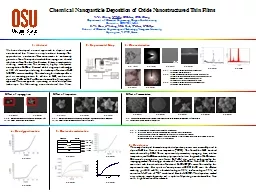
QDrop Behnood G Ghamsari Tamin Tai Steven M Anlage Center for Nanophysics and Advanced Materials Department of Physics University of Maryland Quality Factor Mechanisms
Presentation Embed Code
Download Presentation
Download Presentation The PPT/PDF document "RF Nonlinearity in Thin-Film and Bulk Su..." is the property of its rightful owner. Permission is granted to download and print the materials on this website for personal, non-commercial use only, and to display it on your personal computer provided you do not modify the materials and that you retain all copyright notices contained in the materials. By downloading content from our website, you accept the terms of this agreement.
RF Nonlinearity in Thin-Film and Bulk Superconductors: A Mechanism for Cavity: Transcript
Download Rules Of Document
"RF Nonlinearity in Thin-Film and Bulk Superconductors: A Mechanism for Cavity"The content belongs to its owner. You may download and print it for personal use, without modification, and keep all copyright notices. By downloading, you agree to these terms.
Related Documents