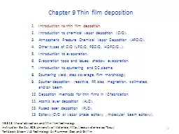
PPT-ALD Thin Film Materials LDRD review 2009
Author : luanne-stotts | Published Date : 2018-09-22
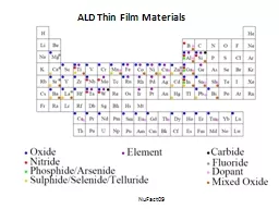
NuFact09 ALD of IIIV semiconductors and other structurematerials What have been done GaN AlN AlGaN InN Not too hard for InGaN TiO 2 ZnO Other Pt nanoparticles
Presentation Embed Code
Download Presentation
Download Presentation The PPT/PDF document "ALD Thin Film Materials LDRD review 2009" is the property of its rightful owner. Permission is granted to download and print the materials on this website for personal, non-commercial use only, and to display it on your personal computer provided you do not modify the materials and that you retain all copyright notices contained in the materials. By downloading content from our website, you accept the terms of this agreement.
ALD Thin Film Materials LDRD review 2009: Transcript
Download Rules Of Document
"ALD Thin Film Materials LDRD review 2009"The content belongs to its owner. You may download and print it for personal use, without modification, and keep all copyright notices. By downloading, you agree to these terms.
Related Documents