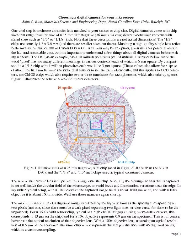
/
chips are actually 4.8 x 3.6 mm (and there are smaller sizes out there chips are actually 4.8 x 3.6 mm (and there are smaller sizes out there

chips are actually 4.8 x 3.6 mm (and there are smaller sizes out there - PDF document

marina-yarberry
marina-yarberry . @marina-yarberry
Follow
407 views
Uploaded On 2016-05-03

chips are actually 4.8 x 3.6 mm (and there are smaller sizes out there - PPT Presentation

allowed among other things for balancing the time for each exposure to compensate for the variation in sensitivity of silicon photodiodes with wavelength But such cameras were slow to operate and ID: 303321

allowed among other things for

Share:

Link:

Embed:

Download Presentation from below link

Download Pdf The PPT/PDF document "chips are actually 4.8 x 3.6 mm (and the..." is the property of its rightful owner. Permission is granted to download and print the materials on this web site for personal, non-commercial use only, and to display it on your personal computer provided you do not modify the materials and that you retain all copyright notices contained in the materials. By downloading content from our website, you accept the terms of this agreement.


Presentation Transcript

chips are actually 4.8 x 3.6 mm (and there are smaller sizes out there). Matching a high-quality single lens reßex body such as the Nikon D80 or Canon EOS 400 to a camera may be an option, given its other potential uses in the lab, and reasonable cost, but it is important to understand a few things about all digital cameras before mak-ing a choice. The D80, as an example, has a 10 million photosites (called individual sensors below, since the word "pixel" has too many different meanings in various contexts) each of which is 6 µm square. By compari-son, in a 1/1.8 chip with 4 million photosites each would be 3 µm square. (These values also allow for a space of about one half µm between the individual sensors to isolate them electrically, and this applies to CCD detec-tors, not CMOS chips which also require two or three transistors for each photosite, which also take up space). Figure 1 illustrates the relative sizes of different detectors. Figure 1. Relative sizes of a 25 mm negative, APS chip (used in digital SLR's such as the Nikon D80), and the "1/1.8" and "1.3" inch chips used in typical consumer cameras.The role of the transfer lens is to project the image onto the chip. Normally the rectangular area that is captured is set well inside the circular Þeld of the microscope, to avoid focus and illumination variations near the edge. In my rather typical setup, with a 10x objective the captured image Þeld is about 1600 µm wide, and with a 100x objective it is about 160 µm wide. We'll use those numbers again shortly.The maximum resolution of a digitized image is deÞned by the Nyquist limit as the spacing corresponding to two pixels (not one, since there must be a dark pixel separating two light ones, or vice versa, for them to be dis-tinguished). For a 3600x2400 sensor chip, typical of a high end 10 Megapixel single-lens-reßex camera, this corresponds to 13 µm on the chip, and for a 10x objective represents 0.9 µm on the specimen. This is, of course, better than the optical resolution of that objective lens. With a 100x objective lens, assuming an optical resolu- allowed, among other things, for balancing the time for each exposure to compensate for the variation in sensi-tivity of silicon photodiodes with wavelength. But such cameras were slow to operate and did not provide a live color image.Another method uses prisms and Þlters that direct the red, green and blue light to three separate detector chips. These cameras are expensive and delicate (the alignment of the chips is critical), are less sensitive (because of the light lost in the optics), and produce color shading with wide angle lenses.Still another technique developed by Foveon fabricates a single chip in which there are three diodes at each photosite, one above the other. Red light penetrates deeper into silicon than blue, so the diode at the surface measures the amount of blue light while Þltering it out. The next diode below it does the same for green, while the red light penetrates to the deepest layer. This method is still somewhat experimental, has thus far been ac-complished only using CMOS technology, and has some problems with the processing needed to obtain accu-rate colors, but has the advantage that every photosite receives the full color information.Figure 3. The Bayer color Þlter array in which one-half of the photosites have a green Þlter, one quarter have a red Þlter, and one quarter a blue Þlter.That is not the case with the most common method of color detection, a color Þlter array (CFA). The most commonly used arrangement is the Bayer Þlter which places red, green and blue Þlters on individual photodi- -lation, along with the use of an "antialiasing" Þlter placed in front of the detector chip to scatter the light and spread the photons out to several sensors, reduces the resolution of the digitized image to about 50% of the value that might be expected from the number of "pixels" advertised in the camera speciÞcation! (Note - there are some camera manufacturers who carry this interpolation much farther, and advertise a number of pixels in the resulting stored image that is many times the number of sensors on the chip.)Silicon photodiodes are inherently linear, so that the output signal from the chip is a direct linear response to the intensity of the incident light. Professional cameras that save the ÒrawÓ information from the chip (which be-cause of the demoisaicing and removal of shot noise is usually not quite the direct photodiode output) do indeed record this linear response. But programs that interpret the raw Þle data to produce viewable images, usually saved as tiff or jpeg formats, apply nonlinear conversions. One reason for this practice is to make the images more like those produced by traditional Þlm cameras, since Þlm responds to light intensity logarithmically rather than linearly.It is also done because of the nature of human vision, which responds to changes in intensity more-or-less loga-rithmically. In a typical scene, a brightness change of a few percent is noticeable. A difference between 20 and 40 (on the 0=black to 255=white scale used by many programs) represents a 100 percent change, while the same absolute difference between 220 and 240 is less than a 10% change.In Þlm photography, images may be recorded on either ÒhardÓ or ÒsoftÓ Þlms and paper. As shown in Figure 4, these are characterized by plots of the density against the log of the incident light intensity that are very steep, producing a high contrast image, or more gradual, covering a greater range of intensity. The slope of the central linear portion of the curve is called the ÒgammaÓ of the Þlm or paper.Figure 4. H & D curves for hard and soft photographic Þlm.The same name is now applied to the same characteristic of digitized images in computer software. Computer displays are nonlinear, with a typical value of gamma in the range from 1.8 (the Macintosh standard) to 2.2 (the Windows standard). The mathematical relationship is Output = Input ^ Gamma (where input and output are normalized to the 0..1 range). To compensate for this nonlinearity, the images may be processed from the cam- with all lossy compression schemes (and even the ones that call themselves ÒlosslessÓ can truncate or round off values) is that there is no way to predict just what details may be eliminated from the original image. Fine lines may be erased, feature boundaries moved, texture eliminated, and colors altered, and this may vary from one image to another and from one location to another within an image. There is no way to recover the lost informa-