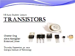
a brief overview Montek Singh Feb 7 12 2018 Transistors as switches At an abstract level transistors are merely switches 3ported voltagecontrolled switch ntype conduct when control input is 1 ID: 760491
Download Presentation The PPT/PDF document "1 COMP541 Transistors and all that…" is the property of its rightful owner. Permission is granted to download and print the materials on this web site for personal, non-commercial use only, and to display it on your personal computer provided you do not modify the materials and that you retain all copyright notices contained in the materials. By downloading content from our website, you accept the terms of this agreement.
Slide1
1
COMP541Transistors and all that…a brief overview
Montek Singh
Feb
{7
, 12}
, 2018
Slide2Transistors as switches
At an abstract level, transistors are merely switches3-ported voltage-controlled switchn-type: conduct when control input is 1p-type: conduct when control input is 0
2
Slide3Silicon as a semiconductor
Transistors are built from siliconPure Si itself does not conduct wellImpurities are added to make it conductingAs provides free electrons n-typeB provides free “holes” p-type
Figure 1.26 Silicon lattice and dopant atoms
Slide4MOS Transistors
MOS = Metal-oxide semiconductor3 terminalsgate: the voltage here controls whether current flowssource and drain: are what the current flows betweenstructurally, source and drain are the same
Figure 1.29
nMOS
and
pMOS
transistors
Slide5nMOS Transistors
Gate = 0OFF = disconnectno current flows between source & drain
Gate = 1ON= connectcurrent can flow between source & drainpositive gate voltage draws in electrons to form a channel
Figure 1.30
nMOS
transistor operation
Slide6nMOS and pMOS Transistors
pMOS: Just the oppositeGate = 1 disconnectGate = 0 connectSummary:
6
Slide7CMOS Topologies
There is actually more to it than connect/disconnectnMOS: pass good 0’s, but bad 1’sso connect source to GNDpMOS: pass good 1’s, but bad 0’sso connect source to VDDTypically use them incomplementary fashion:nMOS network at bottompulls output value down to 0pMOS network at toppulls output value up to 1only one of the two networks must conduct at a time!or output is undefined (or smoke may be produced!)if neither network conducts output will be floating
7
Slide8CMOS Gate Recipe
Use complementary networks of p- and n-transistorscalled CMOS (“complementary metal-oxide semiconductor”)at any time: either “pullup” active, or “pulldown” activenever both!
pullup: make this connectionwhen some combination of inputsis near 0 so that output = VDD
pulldown: make this connectionwhen some combination of inputsis near VDD so that output = 0 (Gnd)
Use
p-type here
Use
n
-type
here
V
DD
Gnd
Slide9CMOS Inverter
V
in
V
out
V
in
V
out
A
Y
inverter
Only a narrow range of input voltages result in
“
invalid
”
output values. (This diagram is greatly exaggerated)
Valid
“
1
”
Valid
“
0
”
Invalid
“
1
”
“
0
”
“
0
”
“
1
”
Slide10CMOS Complements
conducts when A is high
conducts when A is low
conducts when A is high
and
B is high: A
.
B
A
B
A
B
conducts when A is low
or
B is low: A+B = A
.
B
conducts when A is high
or
B is high: A+B
A
B
A
B
conducts when A is low
and
B is low: A
.
B = A+B
A
A
Series N connections:
Parallel N connections:
Parallel P connections:
Series P connections:
Slide11Inverter
11
A
P1
N1
Y
0
ON
OFF
1
1
OFF
ON
0
Slide12NAND
12
A
B
P1
P2
N1
N2
Y
0
0
ON
ON
OFF
OFF
1
0
1
ON
OFF
OFF
ON
1
1
0
OFF
ON
ON
OFF
1
1
1
OFF
OFF
ON
ON
0
Slide133-Input NAND
Slide14NOR
Slide153-input NOR
15
Slide162-input AND Gate?
16
Slide17A More Complex CMOS Gate
Design a single gate that computes Step 1. Determine pull-down network that sets output to ‘0’(A OR B) AND C Y=0Step 2. Determine pull-up network by walking through pulldown hierarchy, andreplacing n-transistors with p-transistorsseries composition with parallel compositionparallel composition with series compositionStep 3. Combine the pull-up and pull-down networks together
C
A
B
C
A
B
C
A
B
C
A
B
Y
Slide18A More Complex CMOS Gate
Single gate that computes called “complex gate” because it is not one of the basic gates (NAND, NOR, NOT, etc.)this one is actually called OR-AND-INVERT (OAI)symbol:
C
A
B
C
A
B
Y
Slide19One More Exercise
Lets construct a gate to compute:F = A+BC = NOT(OR(A,AND(B,C)))Step 1: Draw the pull-down networkStep 2: The complementary pull-up networkthis one is called AND-OR-INVERT (AOI)
F
A
B
C
V
dd
A
B
C
Slide20One More Exercise
Lets construct a gate to compute:F = A+BC = NOT(OR(A,AND(B,C)))Step 1: Draw the pull-down networkStep 2: The complementary pull-up networkStep 3: Combine and Verify
F
A
B
C
V
dd
A
B
C
A
B
C
F
0
0
0
0
0
1
0
1
0
0
1
1
1
0
0
1
0
1
1
1
0
1
1
1
1
1
1
0
0
0
0
0
Slide21Transmission Gates
Transmission gate is a switch:nMOS pass 1’s poorlypMOS pass 0’s poorlyTransmission gate is a better switchpasses both 0 and 1 wellWhen EN = 1, the switch is ON:A is connected to BWhen EN = 0, the switch is OFF:A is not connected to BSymbol:
A
B
En
En
A
B
En
En
Slide22A
B
En
En
Transmission Gate
IMPORTANT
: Transmission gates are not drivers
will NOT remove input noise to produce clean(
er
) output
simply connect A and B
together
current
could even flow backward
!
use
very carefully
!
immediately follow it up with a normal CMOS gate
Slide23Logic using Transmission Gates
Typically combine two (or more) transmission gates Together form an actual logic gate whose output is always driven 0 or 1Exactly one transmission gate drives the output;all remaining transmission gates float their outputsExample: XORwhen C = 0, TG0 conductsF = Awhen C = 1, TG1 conductsF = A’therefore:F = A xor C
23
TG0
TG1
Slide24Tristate buffer and tristate inverter
When enabled: sends input to outputWhen disabled: output is floating (‘Z’)Implementation:Tristate buffer using only a pass gateIf on: output inputIf off: output is floatingTristate inverterTop half and bottom half are not fullycomplementaryEither both conduct: output NOT(input)will act as a driver!Or both off: output is floating
24
Slide25Power and Energy Consumption
25
Slide26Power Consumption
Power = Energy consumed per unit time
Dynamic power consumption
Static power consumption
Slide27Dynamic Power Consumption
Energy consumed due to switching activity:All wires and transistor gates have capacitanceEnergy required to charge a capacitance, C, to VDD is CVDD2Circuit running at frequency f: transistors switch (from 1 to 0 or vice versa) at that frequencyCapacitor is charged f/2 times per secondassume 50% chance switching from 0 to 1additional energy drawn from battery CVDD2assume 50% chance switching from 1 to 0no additional energy taken from battery stored energy is discharged Pdynamic = ½CVDD2f
C
is the total capacitance of circuit (“capacitive load”)
V
DD
is the supply voltage
f
is the switching frequency
Slide28Static Power Consumption
Power consumed when no gates are switchingCaused by the quiescent supply current, IDD (also called the leakage current) Pstatic or Pleakage = IDDVDD
V
DD
is the supply voltage
I
DD
is
the leakage current
Slide29Power Consumption Example
Estimate the power consumption of a wireless handheld computer
V
DD
= 1.2 V
C
= 20
nF
f
= 1 GHz
I
DD
= 20 mA
P
= ½
CV
DD
2
f
+ I
DD
V
DD
=
½(20
nF
)(1.2 V)
2
(1 GHz) + (20 mA)(1.2 V)
= 14.4 W + 24
mW
= 14.424 W