PPT-Structure and Bonding of Carbon and Silicon
Author : mitsue-stanley | Published Date : 2017-03-17
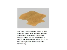
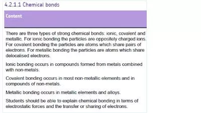
Topic 429 4210 2 characteristics some elements from group 4 are giant molecules carbon and silicon insoluble in almost all solvents h igh melting and boiling
Presentation Embed Code
Download Presentation
Download Presentation The PPT/PDF document "Structure and Bonding of Carbon and Sili..." is the property of its rightful owner. Permission is granted to download and print the materials on this website for personal, non-commercial use only, and to display it on your personal computer provided you do not modify the materials and that you retain all copyright notices contained in the materials. By downloading content from our website, you accept the terms of this agreement.
Structure and Bonding of Carbon and Silicon: Transcript
Download Rules Of Document
"Structure and Bonding of Carbon and Silicon"The content belongs to its owner. You may download and print it for personal use, without modification, and keep all copyright notices. By downloading, you agree to these terms.
Related Documents