/
Circuit Note CN  Circuit Designs Using Analog Devices Products Apply these produ Circuit Note CN  Circuit Designs Using Analog Devices Products Apply these produ

Circuit Note CN Circuit Designs Using Analog Devices Products Apply these produ - PDF document

natalia-silvester
natalia-silvester . @natalia-silvester
Follow
571 views
Uploaded On 2014-10-08

Circuit Note CN Circuit Designs Using Analog Devices Products Apply these produ - PPT Presentation

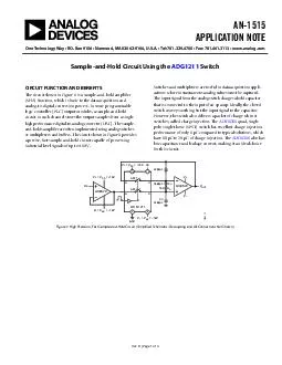
For more information andor support call 1 800 AnalogD 1 800 262 5643 or visit wwwanal ogcomcircuit Devices Connected Referenced ADG1211 Quad SPST Switch with Minimal Charge Injection AD8672 Dual Precision Very Low Noise Operational Ampl ifier Sample ID: 3694

For more information andor

Share:

Link:

Embed:

Download Presentation from below link

Download Pdf The PPT/PDF document "Circuit Note CN Circuit Designs Using A..." is the property of its rightful owner. Permission is granted to download and print the materials on this web site for personal, non-commercial use only, and to display it on your personal computer provided you do not modify the materials and that you retain all copyright notices contained in the materials. By downloading content from our website, you accept the terms of this agreement.


Presentation Transcript

Application Note ��Rev. | Page of TABLE OF CONTENTSCircuit Function and BenefitsRevision HistoryCircuit DescriptionREVISION HISTORY1/201Rev. A to Rev. BDocument Title Changed from CN0058 to AN1515UniversalChanges to Figure 1Rev. 0 to Rev. AUpdated FormatUniversalRevision 0: Initial Version Application Note AN-1515 Rev. B | Page 3 of 3 CIRCUIT DESCRIPTION The circuit shown in Figure 1 is a precise, fast sample-and-hold circuit. During sample mode, SW2 is closed, and the output, VOUTfollows the input signal, V. In hold mode, SW2 is opened, and the signal is held by the hold capacitor, CDue to switch and capacitor leakage current, the voltage on the hold capacitor decays (droops) with time. The ADG1211minimizes this droop due to its low leakage specifications. ADG1211 has 20 pA leakage typically at 25°C and 100 pA maximum. The droop rate is further minimized by the use of a polystyrene hold capacitor. A second switch, SW1, which operates in parallel with SW2, is included in this circuit to reduce pedestal error. Because both switches are at the same potential, they have similar transients, which act as a common-mode signal to the op amp, thereby mini-mizing charge injection effects. Pedestal error is also reduced by the compensation network, R and C. This compensation network also reduces the hold-time glitch and optimizes the acquisition time. The circuit in Figure 1 gives the following results: droop rate of 2 mV/ms, pedestal error of less than 0.5 mV, and acquisition time of 3 ms. The circuit must be constructed on a multilayer printed circuit board with a large area ground plane. Proper layout, grounding, and decoupling techniques must be used to achieve optimum performance (see the MT-031 TutorialMT-088 TutorialMT-090 Tutorial, and MT-101 Tutorial©2009…2018 Analog Devices, Inc. All rights reserved. Trademarks and registered trademarks are the property of their respective owners. AN08625-0-1/18(B) APPLICATION NOTETechnologyWayP.O.Box9106Norwood,02062-9106,U.S.A.Tel:781.329.4700Fax:781.461.3113www.analog.com Sample-and-Hold Circuit Using the Switch Rev. B | Page 1 of 3 CIRCUIT FUNCTION AND BENEFITS The circuit shown in Figure 1 is a sample-and-hold amplifier (SHA) function, which is basic to the data acquisition and analog-to-digital conversion process. In some programmable logic controller (PLC) output modules, a sample-and-hold circuit in each channel stores the output samples from a single high performance digital-to-analog converter (DAC). The sample-and-holds amplifier are often implemented using analog switches or multiplexers and buffers. The circuit shown in Figure 1 provides a precise, fast sample-and-hold circuit capable of processing industrial level signals of up to ±10 V. Switches and multiplexers are useful in data acquisition appli-cations where instantaneous analog values must be captured. The input signal from the analog switch charges a hold capacitor that is connected to the input of an op amp. Ideally, the closed switch conveys nothing but the input signal to the capacitor. However, the switch also delivers a packet of charge when it switches, called charge injection. The ADG1211 quad, single pole, single throw (SPST) switch has excellent charge injection performance of only 1 pC compared to typical solutions, which have 10 pC to 20 pC of charge injection. The ADG1211 also has low capacitance and leakage current, making it an ideal choice for this circuit. 1000pF2200pF V+V– AD8672 SW1SW2 V+ = V = +15VV– = V = –15V AD8672 VIN ADG1211 5 4 13 12 OUT 2200pF = +15VNCV– = V = –15VGND08625-001Figure 1. High Precision, Fast Sample-and-Hold Circuit (Simplified Schematic: Decoupling and All Connections Not Shown)