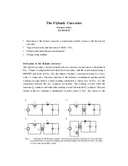
/
Analog-to-Digital Converter (ADC) Analog-to-Digital Converter (ADC)

Analog-to-Digital Converter (ADC) - PowerPoint Presentation

pamella-moone
pamella-moone . @pamella-moone
Follow
686 views
Uploaded On 2015-09-20

Analog-to-Digital Converter (ADC) - PPT Presentation

Introduction to Mechatronics Fall 2012 Craig Woodin Ali AlSaibie Ehsan Maleki Background Information What is ADC Conversion Process Accuracy Examples of ADC applications Presenter Craig ID: 135164

analog adc signal digital adc analog digital signal register conversion input sampling time sequence bit process amp resolution converter approximation registers hold

Share:

Link:

Embed:

Download Presentation from below link

Download Presentation The PPT/PDF document "Analog-to-Digital Converter (ADC)" is the property of its rightful owner. Permission is granted to download and print the materials on this web site for personal, non-commercial use only, and to display it on your personal computer provided you do not modify the materials and that you retain all copyright notices contained in the materials. By downloading content from our website, you accept the terms of this agreement.


Presentation Transcript

Slide1

Analog-to-Digital Converter (ADC)

Introduction to MechatronicsFall 2012Craig WoodinAli AlSaibieEhsan MalekiSlide2

Background Information

What is ADC?Conversion ProcessAccuracyExamples of ADC applicationsPresenter: Craig WoodinSlide3

Signal Types

Analog SignalsAny continuous signal that a time varying variable of the signal is a representation of some other time varying quantityMeasures one quantity in terms of some other quantityExamplesSpeedometer needle as function of speedRadio volume as function of knob movement

tSlide4

Signal Types

Digital SignalsConsist of only two statesBinary StatesOn and offComputers can only perform processing on digitized signals

0

1Slide5

Analog-Digital Converter (ADC)

An electronic integrated circuit which converts a signal from analog (continuous) to digital (discrete) formProvides a link between the analog world of transducers and the digital world of signal processing and data handlingSlide6

Analog-Digital Converter (ADC)

An electronic integrated circuit which converts a signal from analog (continuous) to digital (discrete) formProvides a link between the analog world of transducers and the digital world of signal processing and data handling

tSlide7

Analog-Digital Converter (ADC)

An electronic integrated circuit which converts a signal from analog (continuous) to digital (discrete) formProvides a link between the analog world of transducers and the digital world of signal processing and data handling

tSlide8

ADC Conversion Process

Two main steps of processSampling and HoldingQuantization and Encoding

t

t

Input: Analog Signal

Sampling and Hold

Quantizing

and

Encoding

Analog-to-Digital ConverterSlide9

ADC Process

t

Continuous Signal

Sampling & Hold

Measuring analog signals at uniform time intervals

Ideally twice as fast as what we are sampling

Digital system works with discrete states

Taking samples from each location

Reflects sampled and hold signal

Digital approximationSlide10

ADC Process

t

Sampling & Hold

Measuring analog signals at uniform time intervals

Ideally twice as fast as what we are sampling

Digital system works with discrete states

Taking samples from each location

Reflects sampled and hold signal

Digital approximationSlide11

ADC Process

t

Sampling & Hold

Measuring analog signals at uniform time intervals

Ideally twice as fast as what we are sampling

Digital system works with discrete states

Taking a sample from each location

Reflects sampled and hold signal

Digital approximationSlide12

ADC Process

t

Sampling & Hold

Measuring analog signals at uniform time intervals

Ideally twice as fast as what we are sampling

Digital system works with discrete states

Taking samples from each location

Reflects sampled and hold signal

Digital approximationSlide13

ADC Process

QuantizingSeparating the input signal into a discrete states with K incrementsK=2NN is the number of bits of the ADCAnalog quantization sizeQ=(Vmax-Vmin)/2NQ is the Resolution

Encoding

Assigning a unique digital code to each state for input into the microprocessorSlide14

ADC Process

Quantization & CodingUse original analog signalSlide15

ADC Process

Quantization & CodingUse original analog signalApply 2 bit coding

K=2

2

00

01

10

11

00

11

10

01Slide16

ADC Process

Quantization & CodingUse original analog signalApply 2 bit coding

K=2

2

00

01

10

11

00

11

10

01Slide17

ADC Process

Quantization & CodingUse original analog signalApply 3 bit coding

K=2

3

000

001

010

011

100

101

110

111

Slide18

ADC Process

Quantization & CodingUse original analog signalApply 3 bit coding Better representation of input information with additional bitsMCS12 has max of 10 bits

K=2

3

000

001

010

011

100

101

110

111

K=16

0000

K=…

.

.

.

1111

Slide19

ADC Process-Accuracy

Sampling Rate, TsBased on number of steps required in the conversion processIncreases the maximum frequency that can be measuredResolution, QImproves accuracy in measuring amplitude of analog signal

Limited by the signal-to-noise ratio (~6dB)

t

t

The accuracy of an ADC can be improved by increasing:Slide20

ADC Process-Accuracy

Sampling Rate, TsBased on number of steps required in the conversion processIncreases the maximum frequency that can be measuredResolution (bit depth), QImproves accuracy in measuring amplitude of analog signal

t

t

The accuracy of an ADC can be improved by increasing:Slide21

ADC-Error Possibilities

Aliasing (sampling)Occurs when the input signal is changing much faster than the sample rateShould follow the Nyquist Rule when samplingAnswers question of what sample rate is requiredUse a sampling frequency at least twice as high as the maximum frequency in the signal to avoid aliasingfsample>2*fsignalQuantization Error (resolution)

Optimize resolution

Dependent on ADC converter of

microcontollerSlide22

ADC Applications

ADC are used virtually everywhere where an analog signal has to be processed, stored, or transported in digital formMicrophones Strain Gages ThermocoupleDigital MultimetersSlide23

Types of ADC

Successive Approximation A/D ConverterFlash A/D ConverterDual Slope A/D ConverterDelta-Sigma A/D ConverterPresenter: Ali AlSaibie Slide24

Successive Approximation ADC

ElementsDAC = Digital to Analog ConverterEOC = End of ConversionSAR = Successive Approximation RegisterS/H = Sample and Hold CircuitVin = Input Voltage

Comparator

V

ref

= Reference VoltageSlide25

Successive Approximation ADC

AlgorithmUses an n-bit DAC and original analog resultsPerforms a binary comparison of VDAC and VinMSB is initialized at 1 for DACIf Vin < V

DAC

(V

REF

/

2

^n=1) then MSB is reset to 0If Vin > VDAC (VREF / 2^n) Successive Bits set to 1 otherwise 0Algorithm is repeated up to LSBAt end DAC in = ADC out N-bit conversion requires N comparison cyclesSlide26

Successive Approximation ADC - Example

5-bit ADC, Vin=0.6V, Vref=1VCycle 1 => MSB=1SAR = 1 0 0 0 0VDAC

=

V

ref

/2

^1

= .5 Vin > VDAC SAR unchanged = 1 0 0 0 0Cycle 2SAR = 1 1 0 0 0VDAC = .5 +.25 = .75 Vin < V

DAC SAR bit3 reset to 0 = 1 0 0 0 0Cycle 3SAR = 1 0

1 0 0VDAC = .5 + .125 = .625

V

in

< V

DAC

SAR bit2 reset to 0

= 1 0 0 0

0

Cycle 4

SAR

= 1 0

0

1

0

V

DAC = .5+.0625=.5625 Vin > VDAC SAR unchanged = 1 0 0 1 0Cycle 5SAR = 1 0 0 1 1VDAC = .5+.0625+.03125=

.59375

V

in

>

V

DAC

SAR unchanged =

1 0 0 1

1

Bit

4

3

2

1

0

Voltage

.5

.25

.125

.0625

.03125

DAC bit/voltageSlide27

Flash ADC

Also known as parallel ADCElementsEncoder – Converts output of comparators to binaryComparatorsSlide28

Flash ADC

AlgorithmVin value lies between two comparators Resolution

;

N= Encoder Output bits

Comparators => 2

N

-1

Example:

Vref 8V, Encoder 3-bitResolution = 1.0VComparators 23

-1=71 additional encoder bit -> 2 x # Comparators Slide29

Flash ADC Example

Vin = 5.5V, Vref= 8VVin lies in between Vcomp5 & Vcomp6Vcomp5 =

V

ref

*5/8 =

5V

V

comp6 = Vref*6/8 = 6VComparator 1 - 5 => output 1Comparator 6 - 7 => output 0Encoder Octal Input = sum(0011111) = 5Encoder Binary Output = 1 0 1

5.5V1

11

1

1

0

0Slide30

Dual Slope A/D Converter

Also known as an Integrating ADC

Clock

Counter

Control

Logic

+

_

Start

StopSlide31

Dual-Slope ADC – How It Works

An unknown input voltage is applied to the input of the integrator and allowed to ramp for a fixed time period (tu)

Then,

a known reference voltage of opposite polarity is applied to the integrator and is allowed to ramp until the integrator output returns to

zero (t

d

)

The

input voltage is computed as a function of the reference voltage, the constant run-up time period, and the measured run-down time periodThe run-down time measurement is usually made in units of the converter's clock, so longer integration times allow for higher resolutionsThe speed of the converter can be improved by sacrificing resolutionSlide32

Delta-Sigma A/D Converter

Delta-Sigma Modulator

Analog

Input

Digital

Output

Low-Pass

FilterSlide33

Delta-Sigma ADC – How It Works

Input over sampled, goes to integratorIntegration compared with groundIteration drives integration of error to zeroOutput is a stream of serial bitsSlide34

Comparison of ADC’s

TypeSpeed (relative)Cost(relative)Resolution(bits)Dual Slope

Slow

Med

12-16

Flash

Very

Fast

High4-12Successive ApproxMedium – FastLow8-16Sigma – DeltaSlowLow

12-24Slide35

ADC Subsystem of MC9S12C32

Input Pins

ADC Built-into

MC9S12C32

Presenter: Ehsan Maleki

Slide36

ADC - Schematic Diagram

ATD

Port ADSlide37

ATD 10B8C - Block Diagram

Analog Input

General Purpose I/O

External Trigger

Analog Input

General Purpose I/O

High/Low

Ref Voltage

Power SuppliesSlide38

ATD 10B8C – Key Features

Resolution: 8/10 bitsConversion time: 7 μsec (10 bit)8-channel multiplexed inputsSuccessive Approximation ADCExternal trigger controlConversion Modes:Single or continuous conversionSingle channel or multiple channelsSlide39

Operating Modes

Modes:Stop Mode: All clocks halt; conversion aborts; minimum recovery delay (~ 20μs) Wait Mode: Reduced MCU power; can resumeFreeze Mode: Breakpoint for debugging an applicationSlide40

Registers

MC9S12C Family Reference Manual: Ch. 8REGISTERS6 Control Registers (first 2 are reserved!)2 Status Registers2 Test Registers1 Digital Input Enable Register1 Digital Port Data Register8 Result RegistersSlide41

Control Register (2)

This register controls power down, interrupt, and external trigger.Writes to this register will abort current conversion sequence but will not start a new sequence.

ATD

Power

Interrupt Enable

External Trigger (

Tab. 8-2

)Slide42

Control Register (3)

This register controls the conversion sequence length, FIFO for results registers and behavior in Freeze Mode.Writes to this register will abort current conversion sequence but will not start a new sequence.

Conversion Sequence length

(

Tab. 8-4

)

Background Debug Freeze Enable

(Tab. 8-5)Slide43

Control Register (4)

This register selects the conversion clock frequency, the length of the second phase of the sample time and the resolution of the A/D conversion (i.e.: 8-bits or 10-bits).Writes to this register will abort current conversion sequence but will not start a new sequence.

Resolution

(0=10 bit)

Clock Prescaler

(Default=5)

(Tab. 8-8)Slide44

Control Register (5)

This register selects the type of conversion sequence and the analog input channels sampled.Writes to this register will abort current conversion sequence and start a new conversion sequence.

Result Register Data Justification

RRD Unsigned (0) / Signed (1)

(Tab. 8-10/11)

Single (0) / Continuous (1)

Conversion Mode

Single (0) / Multi (1)

Channel Mode

Analog Input Channel Select

(Tab. 8-12)Slide45

Status Register (0)

This read-only register contains the sequence complete flag, overrun flags for external trigger and FIFO mode, and the conversion counter.

Sequence Complete Flag

Conversion

CounterSlide46

Status Register (1)

This read-only register contains the Conversion Complete Flags.Slide47

Test Registers

Reserved

This register contains the SC bit used to enable special channel conversions.Slide48

Port Data Register

The data port associated with the ATD is general purpose I/O.Slide49

Digital Input Enable Register

This bit controls the digital input buffer from the analog input pin to PTADx data register.Slide50

Results Registers – Left JustifiedSlide51

Results Registers – Right JustifiedSlide52

Step 1: Power up ATD and define settings in

ATDCTL2ADPU = 1 (power up the ATD)ASCIE = 1 (enables interrupt, if needed)Step 2: Wait for ATD recovery time (~ 20μs) Step 3: Set up # of conversions in ATDCTL3Step 4: Configure resolution, sampling time, and ATD clock speed in ATDCTL4Step 5: Configure starting channel, single/multiple channel, single or continuous sequence, and result data format in ATDCTL5

Setting Up & Starting the ADCSlide53

QUESTIONS?Slide54

AppendixSlide55

Table 8-2

BACKSlide56

Tables 8-4 & 8-5

BACKSlide57

Table 8-8Slide58

Table 8-10Slide59

Table 8-11Slide60

Table 8-12Slide61

References

http://en.wikipedia.org/wiki/Analog-to-digital_converterhttp://www.grin.com/object/external_document.259394/fb1fe2e3b955672eca3458c9116d595b_LARGE.pnghttp://en.wikipedia.org/wiki/Successive_approximation_ADChttp://www.maximintegrated.com/app-notes/index.mvp/id/810http://en.wikipedia.org/wiki/Delta-sigma_modulationhttp://www.beis.de/Elektronik/DeltaSigma/DeltaSigma.html

http://www.allaboutcircuits.com/vol_4/chpt_13/9.html

http://en.wikipedia.org/wiki/Integrating_ADC

MC9S12C Family Reference Manual