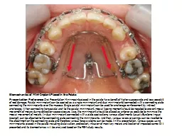
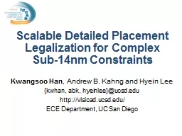
/
Minimum Implant Area-Aware Gate Sizing and Placement Minimum Implant Area-Aware Gate Sizing and Placement

Minimum Implant Area-Aware Gate Sizing and Placement - PowerPoint Presentation

natalia-silvester
natalia-silvester . @natalia-silvester
Follow
441 views
Uploaded On 2016-07-14

Minimum Implant Area-Aware Gate Sizing and Placement - PPT Presentation

Andrew B Kahng and Hyein Lee UC San Diego VLSI CAD Laboratory Minimum Implant Area Constraint Motivation Prior Work Minimum Implant AreaAware Placement and Sizing Experimental Results ID: 403791

placement minia violations sizing minia placement sizing violations implant cells aware area cell minimum heuristic work amp power fix

Share:

Link:

Embed:

Download Presentation from below link

Download Presentation The PPT/PDF document "Minimum Implant Area-Aware Gate Sizing a..." is the property of its rightful owner. Permission is granted to download and print the materials on this web site for personal, non-commercial use only, and to display it on your personal computer provided you do not modify the materials and that you retain all copyright notices contained in the materials. By downloading content from our website, you accept the terms of this agreement.


Presentation Transcript

Slide1

Minimum Implant Area-Aware Gate Sizing and Placement

Andrew B. Kahng and

Hyein Lee

UC

San

Diego VLSI CAD LaboratorySlide2

Minimum Implant Area Constraint

Motivation

Prior WorkMinimum Implant Area-Aware Placement and SizingExperimental ResultsConclusions and Future Work

OutlineSlide3

Implant (active) layers

Regions

for ion implantation (= Vt)Same as the entire cell region

in most cases

Limitation of optical lithography (at λ=193nm) Cannot make small patternsMinimum implant area constraint⇒ A small island of implant layer is not allowed⇒ Challenge for physical design in sub-22nm nodes

Minimum Implant Area (MinIA) Constraint

H

L

L

Minimum implant

width constraint

Violation

<Standard cell layout>

Implant area for P, NMOSSlide4

MUST

consider neighbor cells’ size and

Vt

type

New physical design problems: placement and sizingMotivation: MinIA Constraint in Sub-22nm Nodes

H

MinIA

constraint

WAS: OK

In previous nodes

L

L

Minimum cell size

>

MinIA

constraint

NOW: Violation

In sub-

22nm

nodes

L

L

H

Minimum

cell size

<

MinIA

constraint Slide5

Traditional placement and sizing are separate problems

Placement problem: Place each cell without overlap

Gate sizing problem: Select size and Vt of each cell to minimize power under timing/design constraintsMinIA-aware placement and sizing ⇒ No longer independent of each other in sub-22nm nodes

Sizing needs to understand placement

Example: Changing Vt can create MinIA violations depending on the placementPlacement, sizing and MinIA constraints MUST be considered togetherMotivation: MinIA-Aware Placement and Sizing

L

L

L

H

L

LSlide6

Redefine the traditional placement and gate sizing problems to capture

new

placement, sizing and MinIA rule interactionPropose placement and

sizing

heuristics to optimize power under the MinIA constraintOur proposed methods are implemented in C++ and incorporated into a standard P&R flowOur placement heuristic fixes almost all of violations while commercial tools cannot fix up to 64% of violationsOur sizing and placement heuristic achieves comparable power reduction to the conventional sizing approach without creating MinIA violations

Our WorkSlide7

Gate sizing, and co-optimization with placement

Method to minimize power and ECO cost

Sequential optimization of placement and sizingLinear (1-D) placementGraph model-based approachDynamic programmingLayout effect-aware

placement

STI stress-aware placementNo work considers the MinIA rules in placement and/or sizing Prior Work: LiteratureSlide8

Case study of P&R toolsTechnology:

45nm technology with modified

MinIA rules Commercial P&R tools fix MinIA violations by inserting filler cells Result of two commercial tools

Commercial tools cannot fix all of

MinIA violationsPrior Work: Commercial P&R Tools

50% remaining violationsSlide9

Minimum Implant Area ConstraintMotivationPrior Work

Minimum Implant Area-Aware Placement and Sizing

Experimental ResultsConclusions and Future WorkOutlineSlide10

Problem:

MinIA

-aware sizing and placementMinimize power Subject to:Minimum implant area constraints

Timing

constraints (slack, transition time)No overlap in placementSizing and placement are performed sequentiallyProblem FormulationSlide11

We perform sizing and placement sequentially in our optimizationThree combinations of sizing and placement problems

Free

sizing and MinIA-aware placementAllow MinIA violations and fix the violations later

Strict

MinIA-aware sizingDo not allow any MinIA violations during sizingRelaxed MinIA-aware sizing and MinIA-aware placementAllow fixable MinIA violationsUsed for our optimizerSequential OptimizationSlide12

Levers to solve MinIA

violations

How to Fix MinIA Violations?

H

L

L

H

L

L

H

L

L

L

L

L

<Move neighbor cells>

<Downsize neighbor cells>

<Change

Vt

of cells>

H

L

L

Violation

We must make

the blue area

larger than

MinIA

constraint (

dashed red box

) Slide13

Our Heuristic Flow: Placement

Insert same

V

t

filler cells

around violating cells

V

t

swap the violating cell/

its neighbor cellsto match Vt

Calculate whitespace

for violating cells

Move neighbor cells

to obtain spacing

Insert filler cells

Downsize neighbor cells

to obtain spacing

#

Vio

= 0?

N

finish

#

Vio

= 0?

NY

finish

#

Vio

= 0?

N

Y

finish

Insert filler cells

finish

Y

timing check is neededSlide14

Our Heuristic Flow: Sizing and Placement

Add the cell

to the candidate list

Calculate sensitivity

Pick the most promising cell

And commit

Fix

MinIA

violations

Fixable?

Y

discard

Timing feasible?

N

Y

N

Revert

Sensitivity function =

∆leakage/∆TNS

TNS = total negative slack

TNS is calculated considering sizing and

MinIA

costsSlide15

Our Optimizer

P&R Design (DEF)/LEF

MinIA

-Aware

Placement/Sizing

min implant layer rules

geometry info

def

/lef2oa

Timer Tool/

P&R Tool(DB update,

ECO sizing/placement/

routing)

MinIA

Violation Check

Tcl

socket

OADB

Final P&R Design

Timing update

Apply solutions

s

ave P&R Design

MinIAOptSlide16

Minimum Implant Area ConstraintMotivationPrior Work

Minimum Implant Area-Aware Placement and Sizing

Experimental ResultsConclusions and Future Work

OutlineSlide17

Technology: 45nm technology with modified MinIA

rules

Testcasesdma, mpeg, aes and

jpeg

from OpenCoreHigh utilization (75~82%) is usedMany small cells are used (% of minimum size cells : 59~84%)Additional testcases (aes_var*) with different Vt cell distributionsVarious minimum implant width constraintsExperimental Setup

Testcase

#inst.

Orig. #

Vio

.

dma

1168

193

mpeg

7121

693

aes

9611

1146

jpeg

44911

7864

aes_var1

9611

2955

aes_var2

9611

2558

aes_var3

9611

1816

Const.

Min. width (# sites)

% of violating lib. cells (in a lib.)

Const1

4

3%

Const2

6

12%

Const3

7

28%Slide18

How much MinIA violations can be fixed by our placement heuristic?

Placement results with

Const3

Our approach fixes almost all of violations while commercial tools cannot fix up to 64% of violations

Experimental Results: Placement64% vs. 3%Slide19

Which sizing heuristics show good results w.r.t. both power reduction and MinIA

constraints?

Comparison results between the three heuristicsOur

sizing heuristic

(3) does not increase MinIA violations while maintaining low leakage powerExperimental Results: Sizing and Placement

F

(1) Best leakage reduction

(1) Many

MinIA

violations

(2) Some MinIA violations

(2) Worst leakage reduction

(3) Small

MinIA violations(3) Good leakage reductionSlide20

We address new gate

sizing and

placement problems arising in sub-22nm VLSI due to MinIA constraintWe propose a heuristic sizing and placement method

considering

MinIAOur placement heuristic fixes almost all of violations while commercial tools cannot fix up to 64% of violationsOur sizing and placement heuristic achieves comparable power reduction without creating MinIA violations ConclusionSlide21

Single-row placement with MinIA fixing by using dynamic programming

Unified placement, sizing and

Vt-swap heuristicsMulti-row placement considerationFuture Work

MinIA

violations

H

L

L

H

L

L

H

Standard cell row1

Standard cell row2Slide22

Thank you!