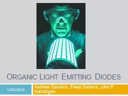
PPT-OLEDs – THEORY AND FABRICATION

Author : natalia-silvester | Published Date : 2017-04-20

ABSTRACT Organic Light Emitting Diodes are quickly becoming the cutting edge in display technology This presentation will give a brief history of OLEDs the theory

Presentation Embed Code

Download Presentation

Download Presentation The PPT/PDF document "OLEDs – THEORY AND FABRICATION" is the property of its rightful owner. Permission is granted to download and print the materials on this website for personal, non-commercial use only, and to display it on your personal computer provided you do not modify the materials and that you retain all copyright notices contained in the materials. By downloading content from our website, you accept the terms of this agreement.

OLEDs – THEORY AND FABRICATION: Transcript


ABSTRACT Organic Light Emitting Diodes are quickly becoming the cutting edge in display technology This presentation will give a brief history of OLEDs the theory behind organic semiconductors the physics behind OLEDs and then go into different fabrication techniques The apparent advantages and disadvantages of OLEDs will also be examined . 1 Introduction CMOS fabrication can be accomplished using either of the three technologies wellP well technologies Twin well technology Silicon On Insulator SOI In this discussion we will focus chiefly on N well CMOS fabrication technology 122 Twin W No TITLES CTP201 Fabrication Of Accident Alert System Using Force Measurement CTP202 Fabrication of Punching Machine With Accident Avoiding System CTP203 Fabrication of Temperature monitoring System In Cutting Tool with Coolant Circulating System CTP Nesibe. . Lakhani. EECS 277A. Prof. Richard Nelson. OLED Structure. OLEDs are . light emitting devices that have a thin film of organic compounds as its emissive electroluminescent layer. . Fabrication Methods. Abstract:. MEMS . technology consists of microelectronic elements, actuators, sensors, and mechanical structures built onto a substrate, which is usually silicon. They are developed using microfabrication techniques: deposition, patterning, and etching. The most common forms of production for MEMS are bulk micromachining, surface micromachining, and HAR fabrication. Fe,Mn. ). 3. O. 4. nanowires using a sidewall deposition method. Tanaka lab. . Takayoshi Kushizaki. M1 colloquium . 8. /6/2011. (. サイドウォール蒸着を用いた. (Fe,Mn). 3. O. 4. ナノワイヤーの作製. Prof Phil Withers. Manchester X-ray imaging Facility. University of Manchester. Volume Scanning. Computer Tomography (CT). The great advantage of computer tomography is that not only do you get the external surface geometry you capture any . Andrew Sanders, . Fawzi. . Salama. , John P. . Handrigan. 12/02/2010. Outline. Introduction. How OLEDs work?. Materials. Fabrication Techniques. Recent Developments. Conclusions. 2. Introduction. 3. DEPARTMENT OF ELECTRONICS & COMMUNICATIONS . NMOS FABRICATION PROCESS. - PROF. RAKESH K. JHA . NMOS FABRICATION PROCESS. Step1. Processing is carried on single crystal silicon of high purity on which required P impurities are introduced as crystal is grown. Such wafers are about 75 to 150 mm in diameter and 0.4 mm thick and they are doped with say boron to impurity concentration of 10 to power 15/cm3 to 10 to the power 16 /cm3.. . Presented at the Fifth International Fab Lab Forum and Symposium on Personal and Digital Fabrication in . Pune. India. . Date: August 16. th. to 22. nd. 2009. . . Introduction:. . The team . E. MITtIng . D. IODE. Display Technology. Jay Dhamsaniya. Rakesh Adroja. Department of E & C Engineering. Institute of Technology. Nirma University. Ahemedabad. OCT . - . 2011. INTRODUCTION. Definition :. ECE 4611. By Sean Davey and Jacob Walker. Image Courtesy of Topper Choice . http://topperchoice.com/working-principle-of-oled-organic-light-emitting-diode/. . In this presentation, we discuss OLED's. How they work, What they are made of, different strategies to manufacture them with layers thicknesses, and the many applications for them.. Lakhani. EECS 277A. Prof. Richard Nelson. OLED Structure. OLEDs are . light emitting devices that have a thin film of organic compounds as its emissive electroluminescent layer. . Fabrication Methods. Fabricating 3D integrated circuits and an overview of the fundamental techniques used.. Samuel Jacobs. EE4611 . 4/5/2017. Overview. 2D vs. 3D integrated circuits. Approaches to manufacturing 3D ICs. Through Silicon . OLED Application to Large Displays OLED technology is the next upcoming display technology. This presentation will cover some OLED basics, different types of OLEDs and the advantages and disadvantages of this technology, as well as some future technologies.

Download Document

Here is the link to download the presentation.
"OLEDs – THEORY AND FABRICATION"The content belongs to its owner. You may download and print it for personal use, without modification, and keep all copyright notices. By downloading, you agree to these terms.

Related Documents