/
Switching Power Supply Topology Voltage Mode vs Switching Power Supply Topology Voltage Mode vs

Switching Power Supply Topology Voltage Mode vs - PDF document

natalia-silvester
natalia-silvester . @natalia-silvester
Follow
600 views
Uploaded On 2014-12-03

Switching Power Supply Topology Voltage Mode vs - PPT Presentation

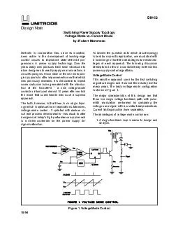
Current Mode by Robert Mammano Unitrode IC Corporation has since its inception been active in the development of leadingedge control circuits to implement stateoftheart pro gressions in power supply technology Over the years many new products have b ID: 20596

Current Mode Robert

Share:

Link:

Embed:

Download Presentation from below link

Download Pdf The PPT/PDF document "Switching Power Supply Topology Voltage ..." is the property of its rightful owner. Permission is granted to download and print the materials on this web site for personal, non-commercial use only, and to display it on your personal computer provided you do not modify the materials and that you retain all copyright notices contained in the materials. By downloading content from our website, you accept the terms of this agreement.


Presentation Transcript

Switching Power Supply TopologyVoltage Mode vs. Current Mode by: Robert MammanoUnitrode IC Corporation has, since its inception,been active in the development of leading-edgecontrol circuits to implement state-of-the-art pro-gressions in power supply technology. Over theyears many new products have been introduced toallow designers to readily apply new innovations incircuit topologies. Since each of these new topolo-gies purports to offer improvements over that whichwas previously available, it is reasonable to expectsome confusion to be generated with the introduc-tion of the UCC3570 - a new voltage-modecontroller introduced almost 10 years after we toldthe world that current-mode was such a superiorapproach.The truth, however, is that there is no single topol-ogy which is optimum for all applications. Moreover,voltage-mode control - if updated with modern cir-cuit and process developments - has much to offerdesigners of today’s high-performance supplies andis a viable contender for the power supply de-signer’s attention.To answer the question as to which circuit topologyis best for a specific application, one must start witha knowledge of both the advantages and disadvan-tages of each approach. The following discussionattempts to do this in a consistent way for these twopower supply control algorithms.Voltage Mode Control This was the approach used for the first switchingregulator designs and it served the industry well formany years. The basic voltage mode configurationis shown in Figure 1. The major characteristics of this design are thatthere is a single voltage feedback path, with pulse-width modulation performed by comparing thevoltage error signal with a constant ramp waveform.Current limiting must be done separately.The advantages of voltage-mode control are:1.A single feedback loop is easier to design andanalyze. Design Note Figure 1. Voltage Mode Control 2.A large-amplitude ramp waveform providesgood noise margin for a stable modulationprocess. 3.A low-impedance power output provides bettercross-regulation for multiple output supplies.Voltage-mode’s disadvantages can be listed as:1.Any change in line or load must first be sensedas an output change and then corrected by thefeedback loop. This usually means slow re-sponse.2.The output filter adds two poles to the controlloop requiring either a dominant-pole low fre-quency roll-off at the error amplifier or anadded zero in the compensation.3.Compensation is further complicated by thefact that the loop gain varies with input voltage.Current Mode ControlThe above disadvantages are relatively significantand since all are alleviated with current-mode con-trol, designers were highly motivated to considerthis topology upon its introduction. As can be seenfrom the diagram of Figure 2, basic current-modecontrol uses the oscillator only as a fixed-frequencyclock and the ramp waveform is replaced with a sig-nal derived from output inductor current.The advantages which this control technique offersinclude the following:1.Since inductor current rises with a slope deter-mined by Vin-Vo, this waveform will respondimmediately to line voltage changes, eliminat-ing both the delayed response and gainvariation with changes in input voltage.2.Since the Error Amplifier is now used to com-mand an output current rather than voltage,the effect of the output inductor is minimizedand the filter now offers only a single pole tothe feedback loop (at least in the normal re-gion of interest). This allows both simplercompensation and a higher gain bandwidthover a comparable voltage-mode circuit.3.Additional benefits with current-mode circuitsinclude inherent pulse-by-pulse current limitingby merely clamping the command from the Er-ror Amplifier, and the ease of providing loadsharing when multiple power units are paral-While the improvements offered by current-modeare impressive, this technology also comes with itsown unique set of problems which must be solvedin the design process. A listing of some of these isoutlined below: Figure 2. Current Mode ControlDesign Note 1.There are now two feedback loops, making cir-cuit analysis more difficult.2.The control loop becomes unstable at duty cy-cles above 50% unless slope compensation is3.Since the control modulation is based on a sig-nal derived from output current, resonances inthe power stage can insert noise into the con-trol loop.4.A particularly troublesome noise source is theleading edge current spike typically caused bytransformer winding capacitance and outputrectifier recovery current.5.With the control loop forcing a current drive,load regulation is worse and coupled inductorsare required to get acceptable cross-regulationwith multiple outputs.So from the above we can conclude that while cur-rent-mode control will ease many of the limitationsof voltage-mode, it also contributes a new set ofchallenges to the designer. However, with theknowledge gained from more recent developmentsin power control technology, a re-evaluation of volt-age-mode control indicated that there werealternative ways to correct its major weaknessesand the result was the UCC3570.Voltage-Mode RevisitedThe two major improvements to voltage-mode con-trol offered by the UCC3570 are voltagefeed-forward to eliminate the effects of line voltagevariations, and higher frequency capability which al-low the poles of the output filter to be placed abovethe range of normal control loop bandwidth.Voltage feed-forward is accomplished by makingthe slope of the ramp waveform proportional to in-put voltage. This provides a corresponding andcorrecting duty cycle modulation with no actionneeded by the feedback loop. The result is a con-stant control loop gain and instantaneous responseto line voltage changes. The higher frequency capa-bility is accomplished through the use of BiCMOSprocessing for this IC which yields smaller parasiticcapacitance and lower circuit delays. Thus many ofthe problems of voltage-mode have been alleviatedwithout incurring the difficulties of current-mode.Choosing Circuit TopologiesNone of the above discussion should leave the im-pression that there is no longer a place forcurrent-mode control - only that both topologies areviable choices in today’s environment. There areconsiderations which could point to one or the otheras more optimum for each particular application.Some of these are outlined below:Consider the use of current-mode if:1.The power supply output is to be a currentsource or very high output voltage.2.The fastest dynamic response is needed witha given switching frequency.3.The application is for a DC/DC converterwhere the input voltage variation is relativelyconstrained.4.Modular applications where parallelability withload sharing is required.5.In push-pull circuits where transformer flux bal-ancing is important.6.In low-cost applications requiring the absolutefewest components.Consider voltage-mode (with feed-forward) if:1.There are wide input line and/or output loadvariations possible.2.Particularly with low line - light load conditionswhere the current ramp slope is too shallow forstable PWM operation.3.High power and/or noisy applications wherenoise on the current waveform would be diffi-cult to control.4.Multiple output voltages are needed with rela-tively good cross-regulation.5.Saturable reactor controllers are to be used asauxiliary secondary-side regulators.6.Applications where the complexities of dualfeedback loops and/or slope compensation isto be avoided.In line with these considerations, the UCC3570 hasbeen optimized for low-to-medium power, off-line,primary-side control applications with isolated feed-back. It features many performance enhancementsfor this task in addition to the control characteristicsdescribed above but, since that is not the purposeof this document, the reader is referred to the prod-uct data sheet for further information.UNITRODE CORPORATION7 CONTINENTAL BLVD. MERRIMACK, NH 03054TEL. (603) 424-2410 FAX (603) 424-3460Reprinted with permission from Electronic Design,June 27, 1994. Copyright 1994, Penton PublishingInc.Design Note IMPORTANT NOTICETexas Instruments and its subsidiaries (TI) reserve the right to make changes to their products or to discontinueany product or service without notice, and advise customers to obtain the latest version of relevant informationto verify, before placing orders, that information being relied on is current and complete. All products are soldsubject to the terms and conditions of sale supplied at the time of order acknowledgement, including thosepertaining to warranty, patent infringement, and limitation of liability.TI warrants performance of its semiconductor products to the specifications applicable at the time of sale inaccordance with TI's standard warranty. Testing and other quality control techniques are utilized to the extentTI deems necessary to support this warranty. Specific testing of all parameters of each device is not necessarilyperformed, except those mandated by government requirements.CERTAIN APPLICATIONS USING SEMICONDUCTOR PRODUCTS MAY INVOLVE POTENTIAL RISKS OFDEATH, PERSONAL INJURY, OR SEVERE PROPERTY OR ENVIRONMENTAL DAMAGE (ÂȘCRITICALAPPLICATIONSÂș). TI SEMICONDUCTOR PRODUCTS ARE NOT DESIGNED, AUTHORIZED, ORWARRANTED TO BE SUITABLE FOR USE IN LIFE-SUPPORT DEVICES OR SYSTEMS OR OTHERCRITICAL APPLICATIONS. INCLUSION OF TI PRODUCTS IN SUCH APPLICATIONS IS UNDERSTOOD TOBE FULLY AT THE CUSTOMER'S RISK.In order to minimize risks associated with the customer's applications, adequate design and operatingTI assumes no liability for applications assistance or customer product design. TI does not warrant or representthat any license, either express or implied, is granted under any patent right, copyright, mask work right, or otherintellectual property right of TI covering or relating to any combination, machine, or process in which suchsemiconductor products or services might be or are used. TI's publication of information regarding any thirdparty's products or services does not constitute TI's approval, warranty or endorsement thereof. 1999, Texas Instruments Incorporated