/
50-500GHz Wireless Technologies: Transistors, ICs, and Systems 50-500GHz Wireless Technologies: Transistors, ICs, and Systems

50-500GHz Wireless Technologies: Transistors, ICs, and Systems - PowerPoint Presentation

nicole
nicole . @nicole
Follow
0 views
Uploaded On 2024-03-15

50-500GHz Wireless Technologies: Transistors, ICs, and Systems - PPT Presentation

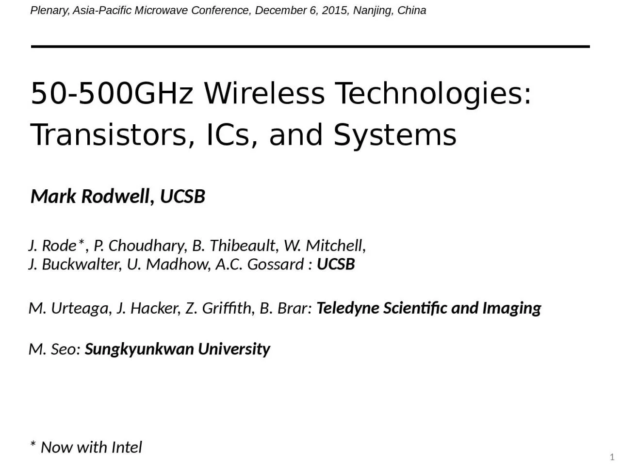
Mark Rodwell UCSB Plenary AsiaPacific Microwave Conference December 6 2015 Nanjing China J Rode P Choudhary B Thibeault W Mitchell J Buckwalter U Madhow AC Gossard ID: 1048512

ghz power base high power ghz high base wave thz inp current ieee seo amp ucsb emitter 2014 series

Share:

Link:

Embed:

Download Presentation from below link

Download Presentation The PPT/PDF document "50-500GHz Wireless Technologies: Transis..." is the property of its rightful owner. Permission is granted to download and print the materials on this web site for personal, non-commercial use only, and to display it on your personal computer provided you do not modify the materials and that you retain all copyright notices contained in the materials. By downloading content from our website, you accept the terms of this agreement.


Presentation Transcript

1. 50-500GHz Wireless Technologies: Transistors, ICs, and Systems Mark Rodwell, UCSBPlenary, Asia-Pacific Microwave Conference, December 6, 2015, Nanjing, ChinaJ. Rode*, P. Choudhary, B. Thibeault, W. Mitchell, J. Buckwalter, U. Madhow, A.C. Gossard : UCSB * Now with IntelM. Seo: Sungkyunkwan UniversityM. Urteaga, J. Hacker, Z. Griffith, B. Brar: Teledyne Scientific and Imaging

2. Why mm-wave wireless ?

3. Links

4. mm-Waves: high-capacity mobile communicationsNeeds→ research: RF front end: phased array ICs, high-power transmitters, low-noise receiversIF/baseband: ICs for multi-beam beamforming, for ISI/multipath suppression, ...

5. mm-Waves: benefits & challengesMassive # parallel channelsNeed mesh networksNeed phased arrays (overcome high attenuation)5Large available spectrumline-of-sight MIMOspatialmultiplexing(note high attenuation in foul weather)

6. mm-Wave LOS MIMO: multi-channel for high capacityTorklinson : 2006 Allerton ConferenceSheldon : 2010 IEEE APS-URSI Torklinson : 2011 IEEE Trans Wireless Comm.

7. Spatial Multiplexing: massive capacity RF networksmultiple independent beams each carrying different data each independently aimed # beams = # array elementsHardware: multi-beam phased array ICs

8. Millimeter-wave imaging 235 GHz video-rate synthetic aperture radar10,000-pixel, 94GHz imaging array→ 10,000 elements Golcuk: Trans MTT, Aug 20141 transmitter, 1 receiver100,000 pixels20 Hz refresh rate5 cm resolution @ 1km50 Watt transmitter (tube, solid-state driver)Demonstrated: SiGe, 1.3 kW (UCSD/Rebeiz)Lower-power designs: InP, CMOS, SiGe (UCSB, UCSD, Virginia Poly.)

9. 140 GHz, 10 Gb/s Adaptive Picocell Backhaul

10. 140 GHz, 10 Gb/s Adaptive Picocell Backhaul350 meters range in 50mm/hr rainPAs: 24 dBm Psat (per element)→ GaN or InPLNAs: 4 dB noise figure → InP HEMTRealistic packaging loss, operating & design margins

11. 340GHz, 160Gb/s spatially multiplexed backhaul600 meters range in 50 mm/hr rain1o beamwidth; 8o beamsteeringPAs: 14 dBm Psat (per element)→ InPLNAs: 7 dB noise figure → InP HEMTRealistic packaging loss, operating & design margins

12. Optimum array size for low system powerAt optimum-size array,target PA output poweris typically 10-200 mW

13. 50-500 GHz Wireless Transceiver ArchitectureIII-V LNAs, III-V PAs → power, efficiency, noiseSi CMOS beamformer→ integration scale...similar to today's cell phones.backhaulendpointHigh-gain antenna → large area→ much too big for monolithic integration

14. Transistors

15. mm-wave CMOS (examples)210 GHz amplifier: 32 nm SOI, positive feedback, 15 dB, 3 stagesWang et al. (Heydari), JSSC, March 2014150 GHz amplifier: 65 nm bulk CMOS, 8.2 dB, 3 stages (250GHz fmax)Seo et al. (UCSB), JSSC, December 2009 300 GHz fmax

16. mm-Wave CMOS won't scale much furtherGate dielectric can't be thinned → on-current, gm can't increaseTungsten via resistances reduce the gainInac et al, CSICS 2011Shorter gates give no less capacitance dominated by ends; ~1fF/mm totalMaximum gm, minimum C→ upper limit on ft. about 350-400 GHz.Present finFETs have yet larger end capacitances

17. III-V high-power transmitters, low-noise receiversCell phones & WiFi:GaAs PAs, LNAsmm-wave links needhigh transmit power, low receiver noise 0.47 W @86GHz0.18 W @220GHz1.9mW @585GHzM Seo, TSC, IMS 2013T Reed, UCSB, CSICS 2013H Park, UCSB, IMS 2014

18. Making faster bipolar transistorsto double the bandwidth:changeemitter & collector junction widthsdecrease 4:1current density (mA/mm2) increase 4:1current density (mA/mm) constantcollector depletion thicknessdecrease 2:1base thicknessdecrease 1.4:1emitter & base contact resistivitiesdecrease 4:1Narrow junctions. Thin layersHigh current densityUltra low resistivity contactsTeledyne: M. Urteaga et al: 2011 DRC

19. THz HBTs: The key challengesObtaining good base contactsin HBT vs. in contact test structure(emitter contacts are fine)Baraskar et al, Journal of Applied Physics, 2013RC parasitics along finger lengthmetal resistance, excess junction areas

20. THz HBTs: double base metal processBlanket surface clean (UV O3 / HCl) strips organics, process residues, surface oxidesBlanket base metal no photoresist; no organic residues Ru refractory diffusion barrier 2 nm Pt : penetrates residual oxidesThick Ti/Au base pad metal liftoff thick metal→ low resistivityRode et al., IEEE TED, Aug. 2015

21. Reducing Emitter Length Effectssmall base post undercutlarge base postbeforeafterlarge base post undercutsmall base post21Rode et al., IEEE TED, Aug. 2015large emitterend undercutsmall emitterend undercut

22. Reducing Emitter Length Effects beforeafterthicker Aubase metalnarrowercollectorjunction22Rode et al., IEEE TED, Aug. 2015

23. InP HBTs: 1.07 THz @200nm, ?? @ 130nm?Rode et al., IEEE TED, Aug. 2015

24. 130nm /1.1 THz InP HBT: ICs to 670 GHz614 GHz fundamentalVCO340 GHz dynamic frequency divider620 GHz, 20 dB gain amplifierM Seo, TSCIMS 2013also: 670GHz amplifierJ. Hacker , TSCIMS 2013 (not shown)M. Seo, TSC / UCSBM. Seo, UCSB/TSCIMS 2010204 GHz static frequency divider(ECL master-slave latch)Z. Griffith, TSCCSIC 2010300 GHz fundamentalPLLM. Seo, TSCIMS 2011220 GHz 180 mWpower amplifier T. Reed, UCSBCSICS 2013600 GHz IntegratedTransmitterPLL + MixerM. Seo TSCIntegrated 300/350GHz Receivers:LNA/Mixer/VCOM. Seo TSC81 GHz 470 mWpower amplifier H-C Park UCSBIMS 2014

25. Towards a 3 THz InP Bipolar TransistorExtreme base doping→ low-resistivity contacts→ high fmaxExtreme base doping→ fast Auger (NP2) recombination→ low b.Solution: very strong base compositional grading→ high b

26. 1/2-THz SiGe HBTs500 GHz fmax SiGe HBTs Heinemann et al. (IHP), 2010 IEDM16-element multiplier array @ 500GHz (1 mW total output)U. Pfeiffer et. al. (Wuppertal / IHP) , 2014 ISSCC

27. Towards a 2 THz SiGe Bipolar TransistorInPSiGeemitter junction width6418nm access resistivity20.6W-mm2base contact width6418nm contact resistivity2.50.7W-mm2collector thickness5315nm current density36125mA/mm2 breakdown2.751.3?Vft10001000GHzfmax20002000GHzSimilar scalingInP: 3:1 higher collector velocitySiGe: good contacts, buried oxidesKey distinction: Breakdown InP has: thicker collector at same ft, wider collector bandgapKey requirements:low resistivity Ohmic contacts note the high current densitiesAssumes collector junction 3:1 wider than emitter.Assumes SiGe contacts no wider than junctions

28. FET scaling laws; 2:1 higher bandwidthchangegate lengthdecrease 2:1current density (mA/mm), gm (mS/mm)increase 2:1transport massconstantgate-channel capacitance densityincrease 2:1contact resistivities decrease 4:1Towards at 2.5 THz HEMTXiaobing Mei, et al, IEEE EDL, April 2015 (Northrop-Grumman)First Demonstration of Amplification at 1 THz Using 25-nm InP High Electron Mobility Transistor ProcessNeed thinner dielectrics, better contacts

29. Towards at 2.5 THz HEMTC. Y. Huang et al., DRC 2015VLSI III-V MOSTHz III-V MOS

30. Power Amplifiers

31. 220 GHz power amplifiers; 256nm InP HBT90 mW180 mW (330 mW design; thermally limited)164 mW, 0.43 W/mm, 2.4% PAET. Reed (UCSB), Z. Griffith (TSC), IEEE CSIC 2012 & 2013; Teledyne 256nm InP HBT

32. mm-Wave Power Amplifier: Challengesneeded: High power / High efficiency / Small die area ( low cost) Extensive power combiningCompact power-combining Efficient power-combining Class E/D/F are poor @ mm-wave insufficient fmax , high losses in harmonic terminations Goal: efficient, compact mm-wave power-combiners

33. Parallel Power-CombiningOutput power: POUT = N x V x I Parallel connection increases POUT Load Impedance: ZOPT = V / (N x I) Parallel connection decreases ZoptHigh POUT→ Low ZoptNeeds impedance transformation: lumped lines, Wilkinson, ...High insertion loss Small bandwidthLarge die area

34. Series Power-Combining & StacksParallel connections: Iout=N x I Series connections: Vout=N x VLocal voltage feedback: drives gates, sets voltage distributionDesign challenge: need uniform RF voltage distribution need ~unity RF current gain per element...needed for simultaneous compression of all FETs.Output power: Pout=N2 x V x ILoad impedance: Zopt=V/ISmall or zero power-combining lossesSmall die areaHow do we drive the gates ?Shifrin et al., 1992 IEEE-IMS; Rodwell et al., U.S. Patent 5,945,879, 1999; Pornpromlikit et al., 2011 CSICS

35. Sub-λ/4 Baluns for Series CombiningSub-l/4 balun : stub→ inductivetunes transistor Cout !short lines→ low lossesshort lines → small dieStandard l/4 balun : long lines→ high losses → large dieBalun combiner:2:1 series connectioneach source sees 25 W→ 4:1 increased PoutPark et al., 2013 CSICS, 2014 IEEE-IMS

36. 2:1 series-connected 86GHz power amplifierDaneshgar et al., 2014 IEEE-IMS20 dB Gain188mW Psat1.96 W/mm32.8% PAETeledyne 250 nm InP HBT2 stages, 1.0 mm2

37. 4:1 series-connected 81GHz power amplifier17 dB Gain470 mW Psat23% PAETeledyne 250 nm InP HBT2 stages, 1.0 mm2(incl pads)Park et al., 2014 IEEE-IMS

38. Teledyne: 1.9 mW, 585 GHz Power AmplifierOutput Power12-Stage Common-base 2.8 dBm Psat>20 dB gain up to 620 GHzWhat limits output power in sub-mm-wave amplifiers ?S-parametersM. Seo et al., Teledyne Scientific: IMS2013

39. Sub-mm-wave PAs: need more current !common-base HBTbaseemittercollectorgroundplaneHBTs with microstrip combiner3 mm max emitter length (> 1 THz fmax)2 mA/mm max current densityImax= 6 mA Maximum 3 Volt p-p output Load: 3V/6mA= 500 WCombiner cannot provide 500 W loading

40. Multi-finger HBTs: more current, lower fmaxMore current→ lower cell load resistanceone-finger common-base HBTtwo-finger power cell four-finger power cell: parasitics baseemittercollectorgroundplanebaseemittercollectorbaseemittercollectorunequal emitter inductancesemitter-collector capacitanceReduced fmax, reduced RF gain:common-lead inductance→ Z12feedback capacitance→ Y12phase imbalance between fingers.Worse at higher frequencies:less tolerant of cell parasiticsless current per cellhigher required load resistanceCan optimum load be reached ?

41. Sub-mm-wave transistors: need more currentInP HBTs:thinner collector→ more currenthotter→ improve heat-sinkingor: longer emitters→ thicker base metalGaN HEMTs: much higher voltage100+ GHz: large multi-finger FETs not feasibleNeed high current to exploit high voltage.Need more mA/mm or longer fingersExample: 2mA/mm, 100 mm max gate width, 50 Volts200mA maximum current50 Volts/200mA= 250 W load→ unrealizable.

42. 50-500GHz Wireless

43. 50-500 GHz Wireless Electronics Mobile communication @ 2Gb/s per user, 1 Tb/s per base stationRequires: large arrays, complex signal processing, high Pout , low FminVLSI beamformersVLSI equalizersIII-V LNAs & PAsIII-V Transistors may perform well enough even for 1 THz systems.

44. (backup slides follow)

45. asdfsadfasdfadsfasdfasdfdfasdf

46. Talk is 40 minplus 10 min for questions…35-40 slides

47. Sub-mm-wave PAs: need more current !<3 mm emitter length for > 1 THz fmax2 mA/mm max current densityImax= 6 mA Maximum 3 Volt p-p output Load: 3V/6mA= 500 WemittercollectorbaseCombiner cannot provide 500 W loadinggroundplane