PDF-Printed in U.S.A., June 1997
Author : pamella-moone | Published Date : 2016-11-24
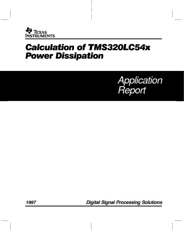
Calculation of TMS320LC54xPower DissipationApplication ReportClay TurnerDigital Signal Processing Solutions
Presentation Embed Code
Download Presentation
Download Presentation The PPT/PDF document "Printed in U.S.A., June 1997" is the property of its rightful owner. Permission is granted to download and print the materials on this website for personal, non-commercial use only, and to display it on your personal computer provided you do not modify the materials and that you retain all copyright notices contained in the materials. By downloading content from our website, you accept the terms of this agreement.
Printed in U.S.A., June 1997: Transcript
Download Rules Of Document
"Printed in U.S.A., June 1997"The content belongs to its owner. You may download and print it for personal use, without modification, and keep all copyright notices. By downloading, you agree to these terms.
Related Documents