PDF-Fabrication Technology
Course Code 3361905
GTU NITTTR Bhopal1
4 1
5
Gujarat State
1
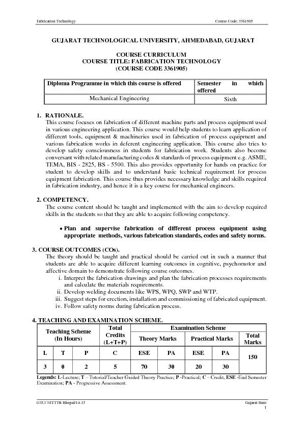
GUJARAT TECHNOLOGICAL UNIVERSITY AHMEDABAD GUJARAT
COURSE CURRICUL
UM
COURSE TITLE FABRICATION TECHNOLOGY
Download Presentation
"Fabrication Technology" is the property of its rightful owner. Permission is granted to download and print materials on this website for personal, non-commercial use only, provided you retain all copyright notices. By downloading content from our website, you accept the terms of this agreement.
Presentation Transcript
Transcript not available.