/
 MEMS Fabrication and Applications  MEMS Fabrication and Applications

MEMS Fabrication and Applications - PowerPoint Presentation

tatiana-dople
tatiana-dople . @tatiana-dople
Follow
348 views
Uploaded On 2020-04-05

MEMS Fabrication and Applications - PPT Presentation

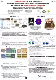
Brought to you by Jack Link amp Aaron Schiller Date delivered on Friday the third of May 2013 ABSTRACT Taking a brief look at MicroElectroMechanical Systems MEMS we will guide you through the fabrication stages and show you some applications that they are used for MEMS can be very simp ID: 775822

mems fabrication www etching mems fabrication www etching sources http deposition applications html sensors show actuators switches source org

Share:

Link:

Embed:

Download Presentation from below link

Download Presentation The PPT/PDF document " MEMS Fabrication and Applications" is the property of its rightful owner. Permission is granted to download and print the materials on this web site for personal, non-commercial use only, and to display it on your personal computer provided you do not modify the materials and that you retain all copyright notices contained in the materials. By downloading content from our website, you accept the terms of this agreement.


Presentation Transcript

Slide1

MEMS Fabrication and Applications

Brought to you by: Jack Link & Aaron SchillerDate delivered on: Friday the third of May, 2013

ABSTRACT:

Taking a brief look at MicroElectroMechanical Systems (MEMS), we will guide you through the fabrication stages and show you some applications that they are used for. MEMS can be very simple and not move at all to being immensely complex systems with lots of moving elements being controlled by the system. Starting off with some simple facts we will then show the stages of their fabrication. The basic process of manufacturing MEMS starts with deposition of thin films onto their respective material layers. Then the material is patterned by one of many forms of lithography. The final step in creating MEMS is etching the pattern so that the final product will be the desired shape. MEMS can be created at a relatively low cost because they can be produced in high volumes because of bulk fabrication. MEMS are used for microvalves for controlling gas and liquid, switches, sensors, actuators, and much more!

Slide2

Outline of our Presentation

A brief overview of MEMS

Fabrication

Basic steps of fabrication

Deposition

Patterning

Etching

Types of Fabrication

Applications

Sensors

Actuators

Switches

Slide3

MEMS and What They Are

MEMS must be mechanically functional whether or not there are any moving partsMEMS devices can be smaller than one um all the way up to several mmReferred to as Microsystems Technology in Europe or Micromachines in JapanUsually consist of a CPU IC that controls the MEMS which act as the eyes and arms of the system.Physics of MEMS are not fully understood

Sources 9 and 5

Slide4

Source 9

Slide5

Fabrication

DepositionManufacturing MEMS starts with depositing a mask on top of a substrateActs as a mechanical layer for the device to built on top ofActs as a "sacrificial layer" and is usually made of some sort of oxidePatterningThe deposition then has a pattern cut out into it to show where it need be etchedDone by some form of lithography, most often photolithography

Sources 1, 5, and 4

Slide6

Fabrication

EtchingWet etching is the most popular amongst MEMS creators because of its fast etch rate and selectivitySubstrate is then dipped in a chemical that will dissolve the deposition but not the mask. Dry etching is much slower and not used as muchDry etching is usually done with either plasma or gas

Sources 1, 4, and 5

Slide7

Start to Finish Picture of the Fabrication of MEMS

Source 1

Slide8

Types of Fabrication

Surface manufacturingAdds deposit to substrate and deposit gets cut awayUsed to make MEMS and IC's on the same silicon waferlayer thickness of around 2 umcomb structures and in-plane operationBulk manufacturingOldest way to create MEMSShaped the way the industry started to make sensors and accelerometers in the 80's and 90'sbetter performance than surfaceHAR (High Aspect Ratio) Siliconlayer thickness of around 10-100umNOT used for IC's, only MEMScombines comb structures and in-plane operation of surface and good performance of bulk

Sources 1 & 5

Slide9

Source 3

Slide10

Uses

Microvalves to control the flow of liquid and gaseous solutionsOptical switches which can change direction, size, and intensity of light beams for displaysMicroactuators which help move large objects easily (e.g. flaps on an airplane)Microsensors which can measure anything from temperature to pressure to radiation.Transducers such as microsensors/actuators which convert energy from one form to another (e.g. depth finder on a boat)

Sources 2 and 5

Slide11

Applications

AccelerometersIn cars tell the airbag to deploy, seatbelts to lock, crash test dummies etc.ElectronicsIn cell phones (e.g. screen rotation), video game controllers, HDD'sMedicalMeasures vitals such as blood pressure, respiration, pulse etc.Eye surgery, inhalers, dialysis, analysis of blood etc.DNA testing

Sources 2 and 5

Slide12

Source 8

Slide13

Above picture: 6

Right picture: 7

Slide14

Summary/Conclusions

MEMS are very useful and can be applied in almost any situation. They are cheap and relatively easy to make and help a lot in everyday life.

Slide15

Sources

1.

https://www.mems-exchange.org/MEMS/fabrication.html

\

2.

https://www.mems-exchange.org/MEMS/applications.html

3.

http://gtresearchnews.gatech.edu/newsrelease/mems-cad.htm

4.

http://www-bsac.eecs.berkeley.edu/projects/ee245/Lectures/lecturepdfs/Lecture2.BulkMicromachining.pdf

5.

http://en.wikipedia.org/wiki/Microelectromechanical_systems

6.

http://www.addonheadrest.com/crashtests.html

7.

http://www.sensorprod.com/dynamic/impact.php

8.

http://www.emeraldinsight.com/journals.htm?articleid=878408&show=html

9.

https://www.mems-exchange.org/MEMS/what-is.html

Slide16

5 Key Concepts

MEMS are always mechanically functional and are usually made from Silicon and silicon dioxide.

Their sizes can range from under one micron to more than several mm.

The three basic steps to fabricating MEMS are deposition, patterning, and etching.

Chemical etching is the primary use of getting the deposition layer because it is easier, faster, and allows finer details

Their main uses are sensors, actuators, and switches