/
15 and 17 September 2021 15 and 17 September 2021

15 and 17 September 2021 - PowerPoint Presentation

payton
payton . @payton
Follow
66 views
Uploaded On 2023-06-23

15 and 17 September 2021 - PPT Presentation

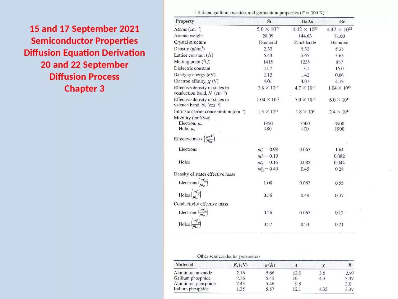
Semiconductor Properties Diffusion Equation Derivation 20 and 22 September Diffusion Process Chapter 3 Doping Using Diffusion Junction Depth 17 In this example Si substrate is ntype doped with the doping concentration ID: 1002332

concentration diffusion type junction diffusion concentration junction type doping process depth surface layer sheet test region resistance wafer silicon

Share:

Link:

Embed:

Download Presentation from below link

Download Presentation The PPT/PDF document "15 and 17 September 2021" is the property of its rightful owner. Permission is granted to download and print the materials on this web site for personal, non-commercial use only, and to display it on your personal computer provided you do not modify the materials and that you retain all copyright notices contained in the materials. By downloading content from our website, you accept the terms of this agreement.


Presentation Transcript

1. 15 and 17 September 2021Semiconductor PropertiesDiffusion Equation Derivation20 and 22 SeptemberDiffusion ProcessChapter 3

2.

3.

4.

5.

6.

7. Doping Using Diffusion

8.

9.

10.

11.

12.

13.

14.

15.

16.

17. Junction Depth17In this example, Si substrate is n-type doped with the doping concentration NB. the diffusion process is to create a p-well in the n-type wafer. N(x) is the p-type doping concentration.xj is the junction depth:x< xj, N(x)> NB, p-type region;x= xj, N(x)= NB, neutral;x> xj, N(x)< NB, n-type region;

18.

19. Lateral Diffusion19During diffusion, impurities not only diffuse vertically, but also move laterally under the edge of any diffusion barrier. Simulation results of two-dimensional diffusion process.

20.

21.

22.

23.

24.

25. The Diffusion Coefficients for Typical Dopants25Diffusion coefficients depend exponentially on temperature:Unit of D: cm2/sec temperature independent term, which depends on the vibration frequency and geometrythe activation energy of the neutral vacancyDiffusion coefficients of typical impurities in SiElement TypeBoron (B)p10.53.69Galliump3.603.51Phosphorusn10.53.69Arsenicn0.323.56

26.

27.

28. Overview of Doping Technologies 28Technology criteria on doping: Doping profile — precise control of doping concentration and region (depth and planar area)Major doping Technologies: High-temperature Diffusion Ion implantation followed by diffusion and annealingDopants (impurities) for Si: n-type dopant (donor): Phosphorus (P), Arsenic (As), Antimony (Sb) p-type dopant (acceptor): Boron (B), Gallium (Ga), Indium (In) Aluminum (Al) not used as a dopant

29. Diffusion with Gas Sources (Phosphorus)292P2O5 + 5Si 5SiO2 +4P2PH3 + 4O2 P2O5 +3H2OThe glass oxide layer is formed on the silicon surface.

30.

31. Diffusion with Liquid Sources (Phosphorus)312P2O5 + 5Si 5SiO2 +4PThe glass oxide layer is formed on the silicon surface.Reactions: 4POCl3 + 3O2 2P2O5 + 6Cl2

32. Diffusion with Solid Sources (Phosphorus)322P2O5 + 5Si 5SiO2 +4PThe glass oxide layer is formed on the silicon surface.Reactions:

33. Reactions for Boron Diffusion33Liquid source: 4BBr3 + 3O2 2B2O3 + 6Br2Boron Diffusion:2B2O3+ 3Si 3SiO2 +4BGas source: 4B2H6 + 3O2 2B2O3 + 3H2O2B2O3+ 3Si 3SiO2 +4BSolid source:4BN + 3O2 2B2O3 + 2N2 2B2O3+ 3Si 3SiO2 +4B

34. Diffusion ProcedureWhat happens during diffusion: Predeposition: deposition of a high concentration of the desired impurity on the silicon surface through windows etched in the protective barrier layer. Drive in: At high temperatures (900 ~ 1200ºC), the impurity atoms move from the surface into the silicon crystal via the substitutional or interstitial mechanisms(b) N-well drive in(a) N-well predepositionPPn-wellSiO2 protective layerDoped regionDoping sourceDoping source removed

35. Mechanisms of Diffusion35Diffusion mechanisms:Si atomImpurity atomSubstitutional diffusionVacancy availableNo vacancy availableInterstitial diffusion The Substitutional diffusion proceeds at a relatively low rate because the supply of vacancies is limited, but this slow diffusion rate is actually an advantage because it permits good control of the diffusion process. The interstitial diffusion mechanism does not require the presence of vacancies, so it proceeds more rapidly than substitutional diffusion. The rapid diffusion rate makes interstitial diffusion difficult to control. Either of the two mechanisms may be dominant depending on process conditions.

36.

37.

38. Lateral Diffusion38During diffusion, impurities not only diffuse vertically, but also move laterally under the edge of any diffusion barrier. Simulation results of two-dimensional diffusion process.

39. Junction Depth39In this example, Si substrate is n-type doped with the doping concentration NB. the diffusion process is to create a p-well in the n-type wafer. N(x) is the p-type doping concentration.xj is the junction depth:x< xj, N(x)> NB, p-type region;x= xj, N(x)= NB, neutral;x> xj, N(x)< NB, n-type region;

40. Junction-Depth Measurement40 Test wafers are normally processed in parallel with the actual IC wafers. The test wafer provides a large area for experimental characterization of junction depth since no making is done on test wafers. Alternatively, special test dice replace a few of the normal die sites on each wafer. These test dice provide an array of test structure for monitoring process and device characteristics during various phases of the process Junction-depth measurement methods: Grove-and-stain method Sheet resistance measurement (four

41. Stanley G. BurnsUMD-ECE

42. Grove-and-stain method42 A cylindrical groove is mechanically ground into the surface of the wafer. After grooving operation, the junction is delineated using a chemical etchant which stains the PN junction. The distance a and b can be measured through a microscope. If radius R of the grinding tool is known. The junction depth is

43. Sheet ResistanceIn diffused layers, resistivity is strong function of depth. In circuit and device design, it is convenient to work with the sheet resistance, Rs Sheet resistance of the layer of material,Unit: ohms per square The ratio (L/W) can be interpreted as the # of unit squares in the resistor.

44. Irwin’s Curve (1) When conductivity varies with the depth of diffusion,andSoxj: the junction depthμ: the majority-carrier mobilityN(x): the net impurity concentrationThe depletion region near the junction xj is neglected.

45. Irwin’s Curve (2) For a given diffusion profile, sheet resistance is uniquely related to the surface concentration of the diffused layer No and the background concentration NB. Sheet resistance is an electrical quantity which depends on the majority-carrier concentration

46. Four-Point Probe (1)46Four-point probe: a special instrument that is used to measure the bulk resistivity of starting wafers and the Rs of shallow diffused layers

47. Principle of Four-Point Probe Measurement47A fixed current is injected into the wafer through the two outer probes, the resulting voltage is measured between the two inner probes.

48. Van der Pauw’s Method48 The sheet resistance of an arbitrary shaped sample of material may be measured by placing four contacts on the periphery of the sample. A current is injected through one pair of the contacts, and the voltage is measured across another pair of contacts.

49. Concentration-Dependent Diffusion49 When the dopant concentration gets higher than certain level, the diffusion becomes concentration-dependent In this case, the Fick’s diffusion equation must account for the concentration-dependent diffusion coefficientFick’s first law of diffusion for 1D diffusion process:D: diffusion coefficient (cm2/s) N: impurity concentration (cm-3)

50. Diffusion in SiO250 SiO2 is frequently used as the mask for diffusion, ion implantation and insulating layer Dopant atoms could also diffuse into SiO2Element TypeBoron (B)p10.53.69Phosphorus (P)n10.53.69Diffusion coefficients in SiElement TypeBoron (B)p3×10-43.53Phosphorus (P)n0.194.03Diffusion coefficients in SiO2