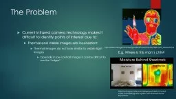
/
Gallium Phosphide as a material for visible and infrared optics Gallium Phosphide as a material for visible and infrared optics

Gallium Phosphide as a material for visible and infrared optics - PDF document

singh
singh . @singh
Follow
342 views
Uploaded On 2022-09-23

Gallium Phosphide as a material for visible and infrared optics - PPT Presentation

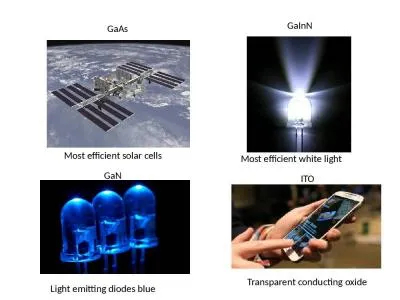
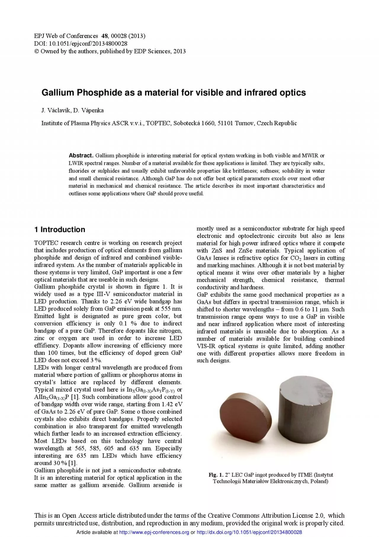
J Václavík 1 D V ápenka 1 1 Institute of Plasma Physics ASCR vvi TOPTEC Sobotecká 1660 51101 Turnov Czech Republic Abstract Gallium phosphide is interesting material for optical sy ID: 955756

gap optical x000b material optical gap material x000b materials production vis refractive range elements produced high x0027 application x001c

Share:

Link:

Embed:

Download Presentation from below link

Download Pdf The PPT/PDF document "Gallium Phosphide as a material for visi..." is the property of its rightful owner. Permission is granted to download and print the materials on this web site for personal, non-commercial use only, and to display it on your personal computer provided you do not modify the materials and that you retain all copyright notices contained in the materials. By downloading content from our website, you accept the terms of this agreement.


Presentation Transcript

Gallium Phosphide as a material for visible and infrared optics J . Václavík 1 , D . V ápenka 1 1 Institute of Plasma Physics ASCR v.v.i., TOPTEC, Sobotecká 1660, 51101 Turnov, Czech Republic Abstract. Gallium phosphide is interesting material for optical system working in both visible and MWIR or LWIR spectral ranges. Number of a material available for these applications is limited. They are typically salts , fluorides or sulphides and usually exhibit unfavorable propert ies like brittleness; softness; solubility in water and small chemical resistance. Although GaP has do not offer best optical parameters excels over most other material in mechanical and chemical resistance. The article describes its most important charact eristics and outlines some applications where GaP should prove useful. 1 Introduction TOPTEC research centre is working on research project that includes production of optical elements from g allium p hosphide and design of infrared and combined visible - infrared system. As the number of materials applicable in those systems is very limited, GaP important is one a few optical materials that are useable in such designs. Gallium p hosphide crystal is shown i n figure 1. It is widely used as a type III - V semiconductor material in LED production. Thanks to 2 . 26 eV wide bandgap has LED produced solely from GaP emission peak at 555 nm. Emitted light is designated as pure green color, but conversion efficiency is only 0.1 % due to indirect bandgap of a pure GaP. Therefore dopants li ke nitrogen, zinc or oxygen are used in order to increase LED effifi ency. Dopants allow increasing of efficiency more than 100 times, but the efficiency of doped green GaP LED does not exceed 3 %. LEDs with longer central wavelength are produced from material where portion of gallium or phosphorus atoms in crystal’s lattice are replaced by different elements. Typical mixed crystal used here is In X Ga (1 - X) As Y P (1 - Y) or AlIn X Ga (1 - X) P [ 1]. Such combinati ons allow good control of bandgap width over wide range , starting from 1.42 eV of GaAs to 2.26 eV of pure GaP. Some o those combined crystals also exhibits direct bandgaps . Properly selected combination is also transparent for emitted wavelength which furt her leads to an increased extraction efficiency. Most LEDs based on this technology have central wavelength at 565, 585, 605 and 635 nm. Especially interesting are 635 nm LEDs which have efficiency around 30 % [1] . Gallium p hosphide is not just a semicondu ctor substrate. It is an interesting material for optical application in the same matter as gallium arsenide. Gallium a rsenide is mostly used as a semiconductor substrate for high speed electronic and optoelectronic circuits but also as lens material for h igh power infrared optics where it compete with ZnS and ZnSe materials. Typical application of GaAs lenses is refractive optics for CO 2 lasers in cutting and marking machines. Although it is not best material by optical means it wins over other materials b y a higher mechanical strength, chemical resistance, thermal conductivity and hardness. GaP exhibits the same good mechanical properties as a GaAs but differs in spectral transmission range, which is shifted to shorter wavelengths – from 0.6 to 11 μm. Such transmission range opens ways to use a GaP in visible and near infrared application where most of interesting infrared materials is unusable due to absorption. As a number of materials available for building combined VIS - IR optical systems is quite limite d, adding another one with different properties allows more freedom in such designs. Fig. 1 . 2” LEC GaP ingot produced by ITME ( Instytut Technologii Materiałów Elektronicznych , Poland) EPJ Web of Conferences Fig. 2 . ZnSe (left) and GaP (rigth) optical elements of bi chromatic lenses for VIS and MWIR application 2 GaP properties Evaluating GaP strictly by optical properties will lead into assumption that there are much better materials actually available. Effectively useable spectral range spans from 570 nm to 11 μm which partially limits its use in visible range. There are other materials covering visible to mid infrared range much better – i.e. ZnS, CaF 2 or BaF 2 . In the infrared end of transmission spectra the GaP losses to materials like ZnSe, BaF 2 or salts like KBr. Fur thermore it exhibits strong dispersion of refractive index in VIS and NIR due to absorption edge at 555 nm. Transmissivity of GaP and other materials from t able 1 is show in figure 3. What makes GaP interesting is combination of its main properties [6] - Tra nsparency from VIS to LWIR - High refractive index - High refractive index dispersion in VIS - Mechanical durability - Verdet constant: 160 rad.m - 1 .T - 1 @ 633 nm Some of its important properties are summarized in t able 1. Average refractive index of GaP is 3.1. It makes GaP material with highest value of refractive index for given transparency in VIS range. It lifts up some constrains in design of fast lenses and optical elements, but it is, in the same time, hampered by strong dispersion of refractive in dex near absorption edge of GaP as is shown in Fig 4. Therefore favorable applications lie in 800 – 1000 nm spectral region which is not part of VIS range but still within sensitivity of Si - based detectors. On the other hand the same dispersion and high refractive index allows design of achromatic pair in combination with ZnSe element. Production example of such lenses is displayed in figure 2. High refractive index requires high quality antireflection coating. So far coatings containing 2 and 4 layers of either SiO 2 - TiO 2 or HfO 2 - ZnS were realized. Antireflection coating were dual - band having minimum reflectivity at 850nm and 4µm. Those coatings were used in VIS - MWIR optics for cutting tool diagnostics. Fig. 3 . Transmissivity of different VIS - IR materials in the range 0.3 - 20µm . [3, 4, 8] Table 1 . Overview of material properties of various optical materials compared to GaP . [ 3, 4, 6 - 1 0 ] GaP GaAs ZnSe ZnS Sapphire CaF 2 BK7 Refractive Index at 1.4µm 3. 16 3.42 2.46 2.28 1.75 1. 43 1.5 Transmissibility at 50% 0. 6 – 11 0. 9 - 16 0. 55 - 19 0. 45 - 11 0.22 - 4. 5 0. 15 – 9 0.33 – 2. 3 Thermooptical Coeficient at (10 - 6 K - 1 ) 100 (at 1.1µm) 250 (at 1.1µm) 59 - 70 (at 1.1µm) 50 (at 1.1µm) 10 (at 0.6µm) - 4 (at 1.1µm) 3 (at 0.6µm) Knoop Hardness (kg.mm - 2 ) 850 750 105 - 120 160 - 220 1700 158 520 Flexural Strength (MPa) 100 55 50 60 500 - 1060 90 50 Fracture Thoughness K IC (MPa.m 1/2 ) 0. 9 0. 4 (orientation - depended) 0.33 - 0. 5 (polycrystali ne) 0,5 3 0.5 0.82 – 1. 1 Price [€/kg] 4500 2200 1800 1400 3000 600 70 Short t itle of the conference Mechanical durability is the most important parameter of the GaP material. Materials with similar transmission range are usually brittle, soft and sensitive to thermal shocks [10] . GaP itself is harder than common optical glass es (BK7), fracture toughness the same or higher than of glass and its flexural strength is also significantly higher. It is insoluble in water and has high acid and alkali resistance. GaP is very durable material compared to commonly used VIS - IR materials li ke BaF 2 , CaF 2 , ZnS, ZnSe, Kbr, KCl. It is suitable as a material for optical elements exposed to mechanical strain, harsh weather conditions or abrasive dust – i.e. windows, cover domes or front elements of optical systems. Fig. 4 . Refractive indices of various VIS - IR materials as a function of wavelength in range 0,6 - 10µm . [3,4] 3 GaP production GaP useable for optical application must be udoped, have minimum of lattice dislocation and minimum free carriers. Free carriers causes b ulk absorption of light in the material at longer wavelength. Minimal specifications for GaP optical material are: - U ndoped material - Carrier concentration: 10 16 cm - 3 - EPD (Etch Pit Density): 5. 10 3 cm - 2 GaP crystal is grown byt LEC (Liquid Encapsulated Czochralski) method. It is well - proven method used by most semiconductor producers to grow III - V semiconductor crystals. Undoped crystals with very high quality, suitable for optical application, are not produced together with material for electronic appli cation. The reason is necessity to fine tune growth a pull process in order to eliminate most of lattice dislocation from produced crystals. Such production is expensive for semiconductor industry. Therefore optical quality GaP is produced by companies spe cialized in growth of optical crystals. Another promising method is VGF (Vertical Gradient Freeze) method which allows control over temperature gradient in crystallization zone. This reduces amount of lattice dislocations and improves optical transmission of the crystal. M arket for optical quality GaP crystals is still small and investment into development of a VGF technology quite large. A uthors do not know any company with successful production using this method. On the other hand there are companies prod ucing quality GaAs crystal s by VGF method. 4 Production of GaP optical elements SPDT is m ost versatile method for processing infrared materials like ZnS , ZnSe or GaAs, but producing optical surfaces for VIS range on GaP is problematic . The TOPEC research centre produces optical elements from GaP with planar and spherical surfaces by optimized grinding - lapping - polishing cycle. Most problematic behavior of GaP is production of phosphine PH 3 whenever phosphorus atoms on the surface can re act with water. PH 3 is very dangerous gas [11 ] and all manufacturing steps must be handled with caution and proper equipment. For a bulk material and surfaces of optical elements it is not a problem, because only a very small portion of phosphorus atoms is exposed. A large surface area is constantly o pened d uring grinding and polishing processes and fresh phosphorus atoms are exposed. Production of PH 3 becomes significant. There are two ways to inhibit production of PH 3 . First is eliminating water from production process – i.e. using alcohols or oils a s replacement of the water in grinding and polishing slurries. Use of oils or alcohols creates serious problem with waste separation and disposal , which increases running costs. Second solution, chosen by t he TOPTEC centre, is use of additives in water bas ed slurries, which causes immediate oxidation of PH 3 dissolved in the slurry. By - product of this process is small amount of phosphorus acid. Grinding and polishing of spherical surfaces on GaP proves to be problematic due to the anisotropy of the crystal a nd etching effects of additives that suppress production of PH 3 . It causes unequal removal rates at different angles and different positions on the surface of produced element. Fig. 5 . MWIR objectives with GaP elements and 47mm aperture produced for GfE - Gesellschaft fuer Fertigungstechnik und Entwicklung e.V., Schmalkalden (Germany) . ��EP- :eb of Conferences 5 Application example Many of the possible applications of GaP material in as an optical element are focused on mixed VIS-IR systems. It could be for example an optical element of thermal imager that needs common optical path for visible and infrared detectors. Let’s have a simpler problem - creating single lens for focusing or collimating laser beam at 1064 nm with smallest possible spot for given focal length. This example was chosen to emphasize importance of very high refractive of this material. As the application is monochromatic a low dispersion materials like CaF do not offer any advantage. Table 2 shows parameters of lenses with EFL = mm, F/3 produced from different materials. Dimensions of the lens and meaning of parameters in the table 2 is closely explained in drawing in figure 6. Shapes of these lenses were calculated in ZEMAX software. It clearly shows that GaP can produce more than six-times smaller focused spot than lens made from C. Example of another lenses produced from GaP is displayed in figure 5. These lenses were produced as objective for MWIR line-scan camera measuring temperature of punching tool. High dispersion of refractive index can be exploited in systems where a compact refractive dispersion element is required. Table 2Comparison of spot sizes and geometric parameters of lenses with EFL = 60 mm and f/3 at λ=1064 nm made from various optical material GaP ZnSe ZnS Saphire CaF 2 BK7 Spot radii (um) 9.5 13.7 15.9 29.7 61.3 49.3 R 1 (mm) 58.47 54.73 52.85 44.1 33.93 36.86 R 2 (mm) 99.53 129. 9 151.7 890.9 - 129.5 - 212.4 Fig. 6. 'imension of laser focusing lens shown as an e[ample of *aP application. 6 Conclusion GaP is member of family of optical materials usable from VIS do 10µm spectral range. As the family does not have many members compared to VIS/NIR and MWIR/LWIR families, specific optical properties gives optical designer another free parameters to solve optical problems. Important characteristic of GaP is its mechanical toughness and chemical resistivity compared to other materials in its family. It was shown that high refractive index in visible range offered by this material can be useful in reducing geometrical aberration. Material releases dangerous substances during mechanical processing and its anisotrop

y leads to irregular removal rates in polishing. TOPTEC research center successfully produces spherical and planar optical elements from GaP and currently works on improvement of manufacturing process.This work was supported by the European Regional 'evelopment Fund and the Ministry of Education,

ls like ZnSe, BaF or salts like KBr. Furthermore it exhibits strong dispersion of refractive index in VIS and NIR due to absorption edge at 555 nm. Transmissivity of GaP and other materials from table 1 is show in figure 3. What makes GaP interesting is combination of its main properties [6] Transparency from VIS to LWIR High refractive index High refractive index dispersion in VIS Mechanical durability Verdet constant: 160 rad.m @ 633 nm Some of important properties are summarized in table 1. Average refractive index of GaP is 3.1. It makes material with highest value of refractive index for given transparency in VIS range. It lifts up some constrains in design of fast lenses and optical elements, but it is, in the same time, hampered by strong dispersion of refractive index near absorption edge of GaP as is shown in Fig 4. Therefore favorable applications lie in 1000 nm spectral region which is not part of VIS range but still within sensitivity of Si-based detectors. On the other hand the same dispersion and high refractive index allows design of achromatic pair in combination with ZnSe element. Production example of such lenses is displayed in figure High refractive index requires high quality antireflection coating. So far coatings containing 2 and 4 layers of either SiO-TiO or HfO-ZnS were realized. Antireflection coating were dual-band having minimum reflectivity at 850nm and 4µm. Those coatings were used in VIS-MWIR optics for cutting tool diagnostics. Fig. 3. Transmissivity of different VIS-IR materials in the range 0.3-20µm. [3, 4, 8] Table 1 . Overview of material properties of various optical materials compared to GaP . [ 3, 4, 6 - 1 0 ] =nSe =nS Sapphire CaF %.7 Refractive Inde[ at 1.4µm 3.42 2.46 2.28 1.75 1.5 Transmissibility at 50 0.22 0.33 Thermooptical Coeficient at 10 at 1.1µm) at 1.1µm) at 1.1µm) at 1.1µm) at 0.6µm) at 1.1µm) at 0.6µm) .noop +ardness kg.mm Fle[ural Strength MPa) 1060 Fracture Thoughness . MPa.m orientation depended) 0.33 polycrystali ne) 0,5 0.5 0.82 Price [€/kg] Gallium Phosphide as a material for visible and infrared optics -. VáclavíkenkaInstitute of Plasma Physics ASCR v.v.i., TOPTEC, Sobotecká 1660, 51101 Turnov, Czech Republic Abstract. *allium phosphide is interesting material for optical system working in both visible and M:IR or L:IR spectral ranges. 1umber of a material available for these applications is limited. They are typically saltsfluorides or sulphides and usually e[hibit unfavorable properties like brittleness softness solubility in water and small chemical resistance. Although *aP has do not offer best optical parameters e[cels over most other material in mechanical and chemical resistance. The article describes its most important characteristics and outlines some applications where *aP should prove useful. Introduction TOPTEC research centre is working on research proMect that includes production of optical elements from gallium phosphide and design of infrared and combined visible-infrared system. As the number of materials applicable in those systems is very limited, *aP important is one a few optical materials that are useable in such designs. *allium phosphide crystal is shown ifigure 1. It is widely used as a type III-V semiconductor material in LE' production. Thanks to 2.26 eV wide bandgap has LE' produced solely from *aP emission peak at 555 nm. Emitted light is designated as pure green color, but conversion efficiency is only 0.1  due to indirect bandgap of a pure *aP. Therefore dopants like nitrogen, zinc or o[ygen are used in order to increase LE' effifiency. 'opants allow increasing of efficiency more than 100 times, but the efficiency of doped green *aP LE' does not e[ceed 3 . LE's with longer central wavelength are produced from material where portion of gallium or phosphorus atoms in crystal’s lattice are replaced by different elements. Typical mi[ed crystal used here is In or AlInP [1]. Such combinations allow good control of bandgap width over wide range, starting from 1.42 of *aAs to 2.26 eV of pure *aP. Some o those combined crystals also e[hibits direct bandgaps. Properly selected combination is also transparent for emitted wavelength which further leads to an increased e[traction efficiency. Most LE's based on this technology have central wavelength at 565, 585, 605 and 635 nm. Especially interesting are 635 nm LE's which have efficiency around 30  [1]. *allium phosphide is not Must a semiconductor substrate. It is an interesting material for optical application in the same matter as gallium arsenide. *allium arsenide is mostly used as a semiconductor substrate for high speed electronic and optoelectronic circuits but also as lens material for high power infrared optics where it compete with =nS and =nSe materials. Typical application of *aAs lenses is refractive optics for CO lasers in cutting and marking machines. Although it is not best material by optical means it wins over other materials by a higher mechanical strength, chemical resistance, thermal conductivity and hardness. *aP e[hibits the same good mechanical properties as a *aAs but differs in spectral transmission range, which is shifted to shorter wavelengths – from 0.6 to 11 μm. Such transmission range opens ways to use a *aP in visible and near infrared application where most of interesting infrared materials is unusable due to absorption. As a number of materials available for building combined VIS-IR optical systems is Tuite limited, adding another one with different properties allows more freedom in such designs. Fig. 1. 2” LEC *aP ingot produced by ITME Instytut Technologii Materiałów Elektronicznych, Poland) EP- :eb of Conferences 5 Application example Many of the possible applications of GaP material in as an optical element are focused on mixed VIS-IR systems. It could be for example an optical element of thermal imager that needs common optical path for visible and infrared detectors. Let’s have a simpler problem - creating single lens for focusing or collimating laser beam at 1064 nm with smallest possible spot for given focal length. This example was chosen to emphasize importance of very high refractive of this material. As the application is monochromatic a low dispersion materials like CaF do not offer any advantage. Table 2 shows parameters of lenses with EFL = mm, F/3 produced from different materials. Dimensions of the lens and meaning of parameters in the table 2 is closely explained in drawing in figure 6. Shapes of these lenses were calculated in ZEMAX software. It clearly shows that GaP can produce more than six-times smaller focused spot than lens made from C. Example of another lenses produced from GaP is displayed in figure 5. These lenses were produced as objective for MWIR line-scan camera measuring temperature of punching tool. High dispersion of refractive index can be exploited in systems where a compact refractive dispersion element is required. Table 2Comparison of spot sizes and geometric parameters of lenses with EFL = 60 mm and f/3 at λ=1064 nm made from various optical material GaP ZnSe ZnS Saphire CaF 2 BK7 Spot radii (um) 9.5 13.7 15.9 29.7 61.3 49.3 R 1 (mm) 58.47 54.73 52.85 44.1 33.93 36.86 R 2 (mm) 99.53 129. 9 151.7 890.9 - 129.5 - 212.4 Fig. 6. 'imension of laser focusing lens shown as an e[ample of *aP application. 6 Conclusion GaP is member of family of optical materials usable from VIS do 10µm spectral range. As the family does not have many members compared to VIS/NIR and MWIR/LWIR families, specific optical properties gives optical designer another free parameters to solve optical problems. Important characteristic of GaP is its mechanical toughness and chemical resistivity compared to other materials in its family. It was shown that high refractive index in visible range offered by this material can be useful in reducing geometrical aberration. Material releases dangerous substances during mechanical processing and its anisotropy leads to irregular removal rates in polishing. TOPTEC research center successfully produces spherical and planar optical elements from GaP and currently works on improvement of manufacturing process.This work was supported by the European Regional 'evelopment Fund and the Ministry of Education,

Effectively useable spectral range spans from 570 nm to 11 μm which partially limits its use in visible range. There are other materials covering visible to mid infrared range much better i.e. ZnS, CaFor BaF. In the infrared end of transmission spectra the GaP losses to materials like ZnSe, BaF or salts like KBr. Furthermore it exhibits strong dispersion of refractive index in VIS and NIR due to absorption edge at 555 nm. Transmissivity of GaP and other materials from table 1 is show in figure 3. What makes GaP interesting is combination of its main properties [6] Transparency from VIS to LWIR High refractive index High refractive index dispersion in VIS Mechanical durability Verdet constant: 160 rad.m @ 633 nm Some of important properties are summarized in table 1. Average refractive index of GaP is 3.1. It makes material with highest value of refractive index for given transparency in VIS range. It lifts up some constrains in design of fast lenses and optical elements, but it is, in the same time, hampered by strong dispersion of refractive index near absorption edge of GaP as is shown in Fig 4. Therefore favorable applications lie in 1000 nm spectral region which is not part of VIS range but still within sensitivity of Si-based detectors. On the other hand the same dispersion and high refractive index allows design of achromatic pair in combination with ZnSe element. Production example of such lenses is displayed in figure High refractive index requires high quality antireflection coating. So far coatings containing 2 and 4 layers of either SiO-TiO or HfO-ZnS were realized. Antireflection coating were dual-band having minimum reflectivity at 850nm and 4µm. Those coatings were used in VIS-MWIR optics for cutting tool diagnostics. Fig. 3. Transmissivity of different VIS-IR materials in the range 0.3-20µm. [3, 4, 8] Table 1 . Overview of material properties of various optical materials compared to GaP . [ 3, 4, 6 - 1 0 ] =nSe =nS Sapphire CaF %.7 Refractive Inde[ at 1.4µm 3.42 2.46 2.28 1.75 1.5 Transmissibility at 50 0.22 0.33 Thermooptical Coeficient at 10 at 1.1µm) at 1.1µm) at 1.1µm) at 1.1µm) at 0.6µm) at 1.1µm) at 0.6µm) .noop +ardness kg.mm Fle[ural Strength MPa) 1060 Fracture Thoughness . MPa.m orientation depended) 0.33 polycrystali ne) 0,5 0.5 0.82 Price [€/kg] EP- :eb of Conferences 5 Application example Many of the possible applications of GaP material in as an optical element are focused on mixed VIS-IR systems. It could be for example an optical element of thermal imager that needs common optical path for visible and infrared detectors. Let’s have a simpler problem - creating single lens for focusing or collimating laser beam at 1064 nm with smallest possible spot for given focal length. This example was chosen to emphasize importance of very high refractive of this material. As the application is monochromatic a low dispersion materials like CaF do not offer any advantage. Table 2 shows parameters of lenses with EFL = mm, F/3 produced from different materials. Dimensions of the lens and meaning of parameters in the table 2 is closely explained in drawing in figure 6. Shapes of these lenses were calculated in ZEMAX software. It clearly shows that GaP can produce more than six-times smaller focused spot than lens made from C. Example of another lenses produced from GaP is displayed in figure 5. These lenses were produced as objective for MWIR line-scan camera measuring temperature of punching tool. High dispersion of refractive index can be exploited in systems where a compact refractive dispersion element is required. Table 2Comparison of spot sizes and geometric parameters of lenses with EFL = 60 mm and f/3 at λ=1064 nm made from various optical material GaP ZnSe ZnS Saphire CaF 2 BK7 Spot radii (um) 9.5 13.7 15.9 29.7 61.3 49.3 R 1 (mm) 58.47 54.73 52.85 44.1 33.93 36.86 R 2 (mm) 99.53 129. 9 151.7 890.9 - 129.5 - 212.4 Fig. 6. 'imension of laser focusing lens shown as an e[ample of *aP application. 6 Conclusion GaP is member of family of optical materials usable from VIS do 10µm spectral range. As the family does not have many members compared to VIS/NIR and MWIR/LWIR families, specific optical properties gives optical designer another free parameters to solve optical problems. Important characteristic of GaP is its mechanical toughness and chemical resistivity compared to other materials in its family. It was shown that high refractive index in visible range offered by this material can be useful in reducing geometrical aberration. Material releases dangerous substances during mechanical processing and its anisotropy leads to irregular removal rates in polishing. TOPTEC research center successfully produces spherical and planar optical elements from GaP and currently works on improvement of manufacturing process.This work was supported by the European Regional 'evelopment Fund and the Ministry of Education,