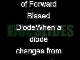
PDF-Capacitance of Forward Biased DiodeWhen a diode changes from reverse b
Author : tatiana-dople | Published Date : 2016-10-25
Charge of Forward Biased Diode PN that will diffuse toward the P region In the P region we have a lot of holes Direction of positive currentDepletion Region
Presentation Embed Code
Download Presentation
Download Presentation The PPT/PDF document "Capacitance of Forward Biased DiodeWhen ..." is the property of its rightful owner. Permission is granted to download and print the materials on this website for personal, non-commercial use only, and to display it on your personal computer provided you do not modify the materials and that you retain all copyright notices contained in the materials. By downloading content from our website, you accept the terms of this agreement.
Capacitance of Forward Biased DiodeWhen a diode changes from reverse b: Transcript
Charge of Forward Biased Diode PN that will diffuse toward the P region In the P region we have a lot of holes Direction of positive currentDepletion Region electron dif. Lecture. 3. 1. Discrete Semiconductor Devices. Semiconductor Materials. Conductor and Insulators.. N-type, P-Type, electron, and hole current. PN junction, depletion region, potential barrier.. Diodes. The inductor has property to store energy . In ac current, during positive high cycle the inductor stores energy . .. Freewheeling diode. At negative half cycle the inductor deenergies ,so there must be reverse current which will make SCR on .. Charge of Forward Biased Diode PN that will diffuse toward the P region In the P region we have a lot of holes Direction of positive currentDepletion Region - - - - - - - - - - electron dif Course . Code : . 11-EC201. DEPARTMENT . OF . ELECTRONICS & COMPUTER . ENGINEERING. Diodes. Contents . Introduction, . Ideal Diode, . Physical Operation of PN Junction Diode,. Terminal Characteristics of Junction Diodes,. CORPORATE INSTITUTE OF SCIENCE . & TECHNOLOGY . , BHOPAL. DEPARTMENT OF ELECTRONICS & COMMUNICATIONS . BY- PROF. RAKESH k. JHA. SCHOTTKY BARRIER DIODE. The Schottky diode (named after German physicist Walter H. Schottky; also known as hot carrier diode) is a semiconductor diode with a low forward voltage drop and a very fast switching action.. (10 MARKS). Visit for more Learning Resources. PN . JUNCTIONDIODE. Biasing of PN junction diode. 1. Forward bias and Reverse bias. . Principle . . If the p-region (anode) is connected to the positive terminal of the external DC source and n-side (cathode) is connected to the negative terminal of the DC source then the biasing is said to be “forward biasing”. . 1. Recap. Three important phenomena occurs during formation of . pn. junction: Diffusion, Formation of Space charge and Drift.. Movement of electrons from n-side to p-side (n>p) and the movement of holes from p-side to n-side is called (p>n) “. A . pn. junction is known as a . semi-conductor . or . crystal . diode. .. The outstanding property of a crystal diode to conduct current in . one direction . only permits it to be used as a rectifier. p-n junction diode. . allows electric current . only. in . forward biased condition. . When forward biased voltage is applied to the p-n junction diode, it allows large amount of electric current. Hence, . is a special type of device designed to operate in the . zener. breakdown region (. reverse breakdown region. ), The breakdown voltage of a . zener. diode is carefully set by controlling the doping level during manufacture. . diode. . is a . p-n junction which . operates only in. . reverse bias. ,. its . capacitance . is varied by varying the reverse . voltage. . The term . varactor. is originated from a variable capacitor. . Zero Biased Junction Diode. When . a diode is connected in a . Zero Bias. condition, no external potential energy is applied to the PN junction. However, if the diodes terminals are shorted together, a few holes (majority carriers) in the P-type material with enough energy to overcome the potential barrier will move across the junction against this barrier potential. This is known as the . & TECHNOLOGY . , BHOPAL. DEPARTMENT OF ELECTRONICS & COMMUNICATIONS . BY- PROF. RAKESH k. JHA. SCHOTTKY BARRIER DIODE. The Schottky diode (named after German physicist Walter H. Schottky; also known as hot carrier diode) is a semiconductor diode with a low forward voltage drop and a very fast switching action.. Pre-labs for ECE 311. Created by Steven . Chambers . in Fall . 2012 . Last Updated: 12/20/2012. Laboratory 0 – Laboratory Demonstration. Introduction to Laboratory 0. Curve Tracer. Plots I-V curve for two and three terminal devices .
Download Document
Here is the link to download the presentation.
"Capacitance of Forward Biased DiodeWhen a diode changes from reverse b"The content belongs to its owner. You may download and print it for personal use, without modification, and keep all copyright notices. By downloading, you agree to these terms.
Related Documents