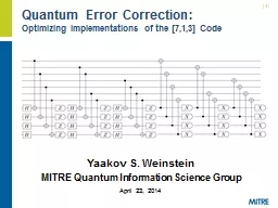
Professor John Kubiatowicz University of California at Berkeley September 28 th 2012 kubitroncsberkeleyedu httpqarccsberkeleyedu Quantum Circuits are Big Some r ecent naïve ID: 424072
Download Presentation The PPT/PDF document "Optimizing the layout and error properti..." is the property of its rightful owner. Permission is granted to download and print the materials on this web site for personal, non-commercial use only, and to display it on your personal computer provided you do not modify the materials and that you retain all copyright notices contained in the materials. By downloading content from our website, you accept the terms of this agreement.
Slide1
Optimizing the layout and error properties of quantum circuits
Professor John KubiatowiczUniversity of California at BerkeleySeptember 28th, 2012 kubitron@cs.berkeley.eduhttp://qarc.cs.berkeley.edu/Slide2
Quantum Circuits are Big!
Some recent (naïve?) estimates for Ground-State Estimation (Level 3 Steane code):209 logical qubits 343 (EC) = 71687 data qubitsTotal operations: 1011 to 1017 (depending on type)
1017
T gates 117,000 ancillas/T gate = 1022 ancillas
51026 Operations for SWAP (communication)And on…Shor’s Algorithm for factoring?5105 or more data
qubits1.5 1015
operations (or more)How can you possibly investigate such circuits?This is the realm of
Computer Architecture and Computer Aided Design (CAD)Slide3
Simple example of Why Architecture Studies are Important (2003)
Consider Kane-style Quantum Computing Datapath
Qubits are embedded P
+ impurities in silicon substrateManipulate Qubit state by manipulating hyperfine interaction with electrodes above embedded impurities
Obviously, important to havean efficient wire For Kane-style technology need sequence of SWAPs to communicate quantum state So – our group tried to figure outwhat involved in providing wire
Results:Swapping control circuit involves complex pulse sequence between every pair of embedded Ions
We designed a local circuit that could swap two Qubits (at < 4K)Area taken up by control was > 150 x area taken by bits!
Conclusion: must at least have a practical WIRE!Not clear that this technology meets basic constraintSlide4
Pushing Limits
Very interesting problems happen at scale!Small circuits become Computer ArchitectureModular designPipeliningCommunication InfrastructureDirect analogies to classical chip design applyThe physical organization of components matters“Wires are expensive, adders are not”?Important Focus Areas for the future:Languages for Describing Quantum
Algorithms
Optimal partitioning and layout Global communication schedulingLayout-driven error correctionSlide5
Expressing QuantumAlgorithmsSlide6
How to express Circuits/Algorithms?
Graphically: Schematic Capture SystemsSeveral of these have been builtQASM: the quantum assembly languagePrimitives for defining single Qubits, GatesC-like languagesScaffold: some abstraction, modules, fixed loopsEmbedded languagesUse languages such as Scala or Ruby to build Domain Specific Language (DSL) for quantum circuitsCan build up circuit by overriding basic operatorsCan introduce a “Reverse” operator to turn classical circuits into reversible quantum onesSlide7
Quantum Circuit model – graphical representation
Time Flows from left to rightSingle Wires: persistent Qubits, Double Wires: classical bitsQubit – coherent combination of 0 and 1: = |0 + |1Universal gate set: Sufficient to form all unitary transformationsExample: Syndrome Measurement (for 3-bit code)
Measurement (meter symbol)
produces classical bitsQuantum CAD Circuit expressed as netlist
Computer manpulated circuitsand implementationsQuantum Circuit ModelSlide8
Higher-Level Language: Chisel
Scala-based language for digital circuit designHigh-level functional descriptions of circuits as inputMany outputs: for instance direct production on VerilogUsed in design of new advanced RISC pipelineFeaturesHigh-level abstractionHierarchical designAbstractions build up circuit (netlist)Inner-Product FIR Digital Filter:Slide9
Quantum Chisel
Simple additions to Chisel Code baseAddition of Classical Quantum translationProduce Ancilla, UseToffoli Gates, CNots, etcReverse Logic to automagically reverse netlists
and produce reversible outputState machine transformation (using “shift registers” to keep extra state when needed)
Because of the way Chisel constructed, can be below the level of syntax (DSL) seen by programmerWith possible exception of explicit REVERSE operatorGoal? Take classical circuits designed in Chisel and produce quantum equivalents
Adders, MultipliersFloating-Point processorsOutput: Quantum Assembly (QASM)Input to other tools!Slide10
One Sticky Issue:Error CorrectionSlide11
Quantum ECC(Concatenated Codes)
Quantum State Fragile encode all QubitsUses many resources: e.g. 343 physical Qubits/logical Qubit)!Need to handle operations (fault-tolerantly)Some set of gates are simply “transversal”: identical operation on each bitOthers (like T gate) much more complex (non-transversal)
Finally, need to perform periodic error correction
Correct after every(?): Gate, Movement, Long Idle PeriodCorrection reducing entropy Consumes Ancilla bits
H
T
Not Transversal!
n-physical Qubits
per logical Qubit
H
T
X
Encoded
/8 (T)
Ancilla
SX
T:
Correct
Correct
Correct
Correct
Correct
Correct
Correct
Correct
QEC
Ancilla
Correct
Errors
Correct
Syndrome
ComputationSlide12
Topological (Surface) Quantum ECC
Physical Qubits on links in the latticeContinuous Measurement and CorrectionMeasuring stabilizers (groups of 4) yields error syndromesOptimizations around the decoding algorithm and frequency of measurement
Rough boundary
Smooth boundarySlide13
Computation with Topological Codes
Each logical Qubit represented by a pair of holesLayout for Large Algorithm: Tile Lattice with paired holesCNOT: move a smooth hole around a rough oneComplications: may need to transform a smooth hole into a rough one before performing CNOT
Rules for how to move holes (grow and shrink them)
Again: Some gates easy, some not (Once again, T is messy)Slide14
Moving to the Realmof
Quantum Computer Aided DesignSlide15
Need for
CAD: More than just SizeData locality:Where qubits “live” and how they move can make or break the ability of a quantum circuit to function:Movement carries risk and consumes timeAncilla must be created close to where usedCommunication must be minimized through routing optimizationCustomized (optimal?) data movement customized channel structure/quantum data
pathOne-size fits all topology not necessarily the best
Parallelism:How to exploit parallelism in dataflow graphPartitioning and scheduling algorithmsArea-Time tradeoff in Ancilla
generationCustomized circuits for pre-computing non-transversal Ancilla reuse?Error Correction:One-size fits all probably not desirableAdapt level of encoding in circuit-dependent way
Corrections after every operation may not be necessarySlide16
Classical Control
Teleportation Network
Quadence Design Tool
Schematic Capture
(Graphical Entry)
Quantum Assembly
(QASM)
OR
QEC Insertion
Partitioning
Layout
Network Insertion
Error Analysis
…
Optimization
CAD Tool
Implementation
Custom Layout and
SchedulingSlide17
Important Measurement Metrics
Traditional CAD Metrics:AreaWhat is the total area of a circuit?Measured in macroblocks (ultimately m2 or similar)Latency (Latencysingle)
What is the total latency to compute circuit once
Measured in seconds (or s)Probability of Success (P
success)Not common metric for classical circuitsAccount for occurrence of errors and error correctionQuantum Circuit Metric: ADCR Area-Delay to Correct Result: Probabilistic Area-Delay metric
ADCR = Area E(Latency) =
ADCR
optimal: Best ADCR over all configurationsOptimization potential: Equipotential designs
Trade Area for lower latencyTrade lower probability of success for lower latencySlide18
Quantum CAD flow
QEC InsertCircuitSynthesisHybrid FaultAnalysis
Circuit
Partitioning
Mapping,Scheduling,Classical control
Communication
Estimation
Teleportation
NetworkInsertion
Input Circuit
Output Layout
ReSynthesis (ADCR
optimal
)
P
success
Complete Layout
ReMapping
Error Analysis
Most Vulnerable Circuits
Fault-Tolerant
Circuit
(No layout)
Partitioned
Circuit
Functional
System
QEC
Optimization
Fault
Tolerant
ADCR computationSlide19
Optimizing Ancilla and LayoutSlide20
An Abstraction of Ion Traps
Basic block abstraction: Simplify LayoutEvaluation of layout through simulationMovement of ions can be done classically
Yields Computation Time and Probability of Success
Simple Error Model: Depolarizing ErrorsErrors for every Gate Operation and Unit of WaitingBallistic Movement Error: Two error ModelsEvery Hop/Turn has probability of error
Only Accelerations cause error
in/out ports
straight
3-way
4-way
turn
gate locationsSlide21
Example Place and Route Heuristic:
Collapsed Dataflow
Gate locations placed in dataflow order
Qubits flow left to right
Initial dataflow geometry folded and sorted
Channels routed to reflect dataflow edges
Too many gate locations, collapse dataflow
Using scheduler feedback, identify latency critical edges
Merge critical node pairs
Reroute channels
Dataflow mapping allows pipelining of computation!
q0
q1
q2
q3
q0
q1
q2
q3
q0
q1
q2
q3Slide22
Quantum Logic Array (QLA)
Anc
Comp
Anc
Comp
Anc
Comp
Anc
Comp
Anc
Comp
Anc
Comp
Anc
Comp
Anc
Comp
Anc
Comp
TP
EPR
EPR
EPR
EPR
EPR
EPR
EPR
EPR
EPR
EPR
EPR
EPR
TP
TP
TP
TP
TP
EPR
EPR
EPR
Correct
Correct
1 or 2-Qubit
Gate (logical)
Storage for
2 Logical Qubits
(In-Place)
n-physical
Qubits
Syndrome
Ancilla
Factory
Correct
Basic Unit:
Two-Qubit cell (logical)
Storage, Compute, Correction
Connect Units with Teleporters
Probably in mesh topology, but
details never entirely clear from original papers
First Serious (Large-scale) Organization (2005)
Tzvetan S. Metodi, Darshan Thaker,
Andrew W. Cross, Frederic T. Chong, and Isaac L. Chuang
Teleporter
NODE
EPR
EPR
EPR
EPRSlide23
Parallel Circuit Latency
Running Circuit at “Speed of Data”
Often,
Ancilla
qubits
are independent of data
Preparation may be pulled offline
Very clear Area/Delay tradeoff:
Suggests Automatic Tradeoffs (CAD Tool)Ancilla qubits
should be ready “just in time” to avoid ancilla decoherence from idleness
H
C
X
H
T
T
QEC
QEC
QEC
QEC
QEC
QEC
T-Ancilla
T-Ancilla
Q0
Q1
QEC
Ancilla
QEC
Ancilla
QEC
Ancilla
QEC
Ancilla
QEC
Ancilla
QEC
Ancilla
Hardware Devoted to
Parallel Ancilla Generation
Serial Circuit LatencySlide24
How much Ancilla Bandwidth Needed?
32-bit Quantum Carry-
Lookahead
Adder
Ancilla use very uneven (e.g. zero and T ancilla)Performance is flat at high end of ancilla generation bandwidth
Can back off 10% and save orders of magnitude in areaMany bits idle at any one time
Need only enough ancilla to maintain state for these bits
Many not need to frequently correct idle errorsConclusion: makes sense to compute ancilla
requirements and share area devoted to ancilla generationCan precompute ancilla for non-transverse gates!Slide25
Tiled Quantum Datapaths
Several Different Datapaths mappable by our CAD flowVariations include hand-tuned Ancilla generators/factoriesMemory: storage for state that doesn’t move muchLess/different requirements for AncillaOriginal CQLA paper used different QEC encoding Automatic mapping must:Partition circuit among compute and memory regionsAllocate Ancilla resources to match demand (at knee of curve)Configure and insert teleportation network
Anc
Comp
Anc
Comp
Anc
Comp
Anc
Comp
Anc
Comp
Anc
Comp
Anc
Comp
Anc
Comp
Anc
Comp
EPR
EPR
EPR
EPR
EPR
EPR
EPR
EPR
EPR
EPR
EPR
EPR
TP
TP
TP
TP
Previous: QLA,
LQLA
Anc
Mem
Anc
Mem
Anc
Comp
Anc
Comp
Anc
Comp
Anc
Mem
Anc
Mem
Anc
Mem
Anc
Mem
TP
TP
TP
TP
EPR
EPR
EPR
EPR
EPR
EPR
EPR
EPR
EPR
EPR
EPR
EPR
Previous: CQLA,
CQLA+
TP
Anc
Comp
Anc
Anc
Mem
Anc
Comp
Anc
Mem
Anc
Mem
TP
TP
EPR
EPR
EPR
EPR
EPR
EPR
EPR
EPR
Anc
Comp
Our Group:
QalypsoSlide26
Which
Datapath is Best?Random Circuit GenerationSplitting factor (r): measures
connectivity of the circuitRelated to Rent’s factor
Qalypso clear winner 4x lower latency than LQLA2x smaller area than CQLA+Why Qalypso does well:Shared, matched
ancilla factoriesAutomatic network sizing (rather than fixed teleportation)Automatic Identification of Idle Qubits (memory)LQLA and CQLA+ perform close secondOriginal supplemented with better ancilla generators, automatic network sizing, and Idle Qubit identification
Original QLA and CQLA do very poorly for large circuitsSlide27
Optimizing
Error CorrectionSlide28
Reducing QEC Overhead
Standard idea: correct after every gate, and long communication, and long idle timeThis is the easiest for people to analyzeThis technique is suboptimalNot every bit has same noise level!Different idea: identify critical QubitsTry to identify paths that feed into noisiest output bitsPlace correction along these paths to reduce maximum noise
H
H
Correct
Correct
Correct
Correct
Correct
Correct
Correct
H
H
CorrectSlide29
QEC Optimization
Modified version of retiming algorithm: called “recorrection:”Find minimal placement of correction operations that meets specified MAX(EDist) EDistMAXProbably of success not always reduced for EDistMAX > 1
But, operation count and area drastically reduced
Use Actual Layouts and Fault AnalysisOptimization pre-layout, evaluated
post-layout
EDist
MAX
iteration
QEC
OptimizationEDistMAX
Partitioning
andLayout
Fault
Analysis
Optimized
Layout
Input
Circuit
1024-bit QRCA and QCLA addersSlide30
Recorrection of 500-gate
Random Circuit (r=0.5)Not all codes do equally well with RecorrectionBoth [[23,1,7]] and [[7,1,3]] reasonable candidates[[25,1,5]] doesn’t seem to do as wellCost of communication and Idle errors is clear here!However – real optimization situation would vary EDist to find optimal point
Probability of Success
Move Error Rate per Macroblock
EDist
MAX
=3
Probability of Success
Idle Error Rate per CNOT Time
EDist
MAX
=3Slide31
Investigating LargerCircuitsSlide32
What does Quadence do?
ECC Insertion and OptimizationLogical Physical circuitsIncludes encoding, and correctionECC Recorrection optimization (more later) Circuit partitioningFind minimum places to cut large circuitCompute ancilla needsPlace physical qubits in proper regions of grid
Communication Estimation and insertionGenerate Custom Teleportation network
Schedule movement of bitsMovement within Ancilla generators (Macros)Movement within compute and memory regionsMovement two and from teleportation stationsSimulation of result to get timing for full circuit
MonteCarlo simulation to get error analysisSlide33
Possible 1024-bit adders
Quantum Ripple-Carry adder (QRCA)Tradeoffs between area and parallelismOr – between speed and circuit reuseSubadder: m-bit QRCAQuantum Carry-Lookahead adder (QCLA)Stronger tradeoff between area and parallelismArity of carry-lookaheadSubadder: m-bit QCLASlide34
Comparison of 1024-bit adders
Carry-Lookahead is better in all architecturesQEC Optimization improves ADCR by order of magnitude in some circuit configurations
ADCR
optimal
for
1024-bit QCLA
ADCR
optimal
for
1024-bit QRCA and QCLASlide35
Error Correction is
not predominant use of areaOnly 20-40% of area devoted to QEC ancillaFor Optimized Qalypso QCLA, 70% of operations for QEC ancilla generation, but only about 20% of areaT-Ancilla generation is major componentOften overlookedNetworking is significant portion of area when allowed to optimize for ADCR (30%)CQLA and QLA variants didn’t really allow for much flexibility
Area Breakdown for AddersSlide36
Direct Comparison:Concatenated and Topological QECCSlide37
Ground State Estimation
Ground State Estimation Find ground state of Glycine Problem Size:50 Basis FunctionsResult Calculated with 5 Bits accuracy60 Qubits, 6.9 x 10¹² gates, Parallelism: 2.5Conceptual PrimitivesQuantum Simulation and Phase Estimation
C
C
O
N
H
H
H
H
HSlide38
Properties of Quantum Technologies: Gate Times and Errors
Ion traps slower but more reliable than superconductorsNeutral atoms unusable with concat. codes
Supercond
.
Qubits
(Primitive)
Supercond
.
Qubits (Optimal)
Ion Traps (Primitive)
Ion Traps (Optimal)
Neutral Atoms (Primitive)
Neutral Atoms (Trotter)
Time (ns)
25
28
32,000
32,000
14,818
19,465
Gate Err
1.0x10
-5
6.6x10
-4
3.2x10
-9
2.9x10
-7
8.1x10
-3
1.5x10
-3
Mem
Err
1.0x10
-5
1.0x10
-5
2.5x10
-12
2.5x10
-12
0.0
0.0Slide39
Ground State Estimation, Multiple Technologies
39
Neutral Atoms (Trotter)
Supercond
.
Qubits
(Primitive)
Ion Traps (Primitive)
Surface Code
10,883 years
4.5 years
5,588 years
Time
2.0 x 10
24
3.5 x 10
22
3.9 x 10
22
Gates
2.5 x 10
8
1.7 x 10
7
4.4 x 10
7
Qubits
Bacon
Shor
Code
-
4,229 years
128 years
Time
-
9.5 x 10
32
1.5 x 10
19
Gates
-
9.4 x 10
11
1.6 x 10
5
Qubits
-
5
1
Concatenations
1 x 10
-3
19,000 ns
1 x 10
-5
25 ns
1 x 10
-9
32,000
nsSlide40
Conclusion
How to express quantum algorithms?Embedded DSLs in higher-order languagesSize of Quantum Circuits Must Optimize Locality Presented Some details of a Full CAD flow (Partitioning, Layout, Simulation, Error Analysis)New Evaluation Metric: ADCR = Area E(Latency)Full mapping and layout accounts for communication cost Ancilla Optimization ImportantAncilla
bandwidth varies widelyCustom
ancilla factories sized to meet needs of circuit“Recorrection
” Optimization for QECSelective placement of error correction blocksValidation with full layout to find optimal level of correctionAnalysis of 1024-bit adder architecturesCarry-Lookahead adders better than Ripple Carry adders
Error correction not the primary consumer of area!