/
The ADA4302-4 features four differential outputs. The differential arc The ADA4302-4 features four differential outputs. The differential arc

The ADA4302-4 features four differential outputs. The differential arc - PDF document

tatiana-dople
tatiana-dople . @tatiana-dople
Follow
457 views
Uploaded On 2015-10-30

The ADA4302-4 features four differential outputs. The differential arc - PPT Presentation

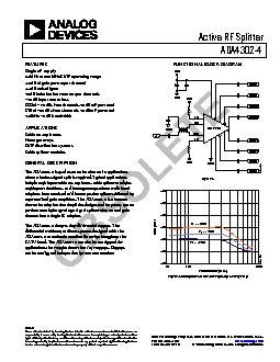
FUNCTIONAL BLOCK DIAGRAM SPLITTERVINILPVIPILNGNDGNDJ1GNDVCC VCC VOP1 05017016 VON4 Figure 1 ADA43024 Rev B Page 8 of 12 APPLICATIONS The ADA43024 active splitter is primarily intended fo ID: 176956

FUNCTIONAL BLOCK DIAGRAM SPLITTERVINILPVIPILNGNDGNDJ1GNDVCC VCC VOP1 05017-016 VON4 Figure

Share:

Link:

Embed:

Download Presentation from below link

Download Pdf The PPT/PDF document "The ADA4302-4 features four differential..." is the property of its rightful owner. Permission is granted to download and print the materials on this web site for personal, non-commercial use only, and to display it on your personal computer provided you do not modify the materials and that you retain all copyright notices contained in the materials. By downloading content from our website, you accept the terms of this agreement.


Presentation Transcript

Active RF Splitter ADA4302-4 Rev. B Information furnished by Analog Devices is believed to be accurate and reliable. However, no responsibility is assumed by Analog Devices for its use, nor for any infringements of patents or other rights of third parties that may result from its use. Specifications subject to change without notice. No license is granted by implication or otherwise under any patent or patent rights of Analog Devices. Trademarks and registered trademarks are the property of their respective owners. One Technology Way, P.O. Box 9106, Norwood, MA 02062-9106, U.S.A.Tel: 781.329.4700 www.analog.com SPLITTERVINILPVIPILNGNDGNDJ1GNDVCC VCC + VCC VOP4 VON3 VOP3 VON2 VOP2 VON1 VOP1 05017-016 VON4 Figure 1. 05017-008 OBSOLETE –70100 –60–65–75–80 =–40 TA = +25C Figure 2. Composite Second-Order (CSO) vs. Frequency ADA4302-4 Rev. B | Page 2 of 12 TABLE OF CONTENTS Features..............................................................................................1Applications.......................................................................................1General Description.........................................................................1Functional Block Diagram..............................................................1Revision History...............................................................................2Specifications.....................................................................................3Absolute Maximum Ratings............................................................4ESD Caution..................................................................................4Pin Configuration and Function Descriptions.............................5Typical Performance CharacteristicsApplicationsCircuit DescriptionEvaluation BoardsRF Layout ConsiderationsPower SupplyOutline Dimensions.......................................................................11Ordering Guide..........................................................................11REVISION HISTORY 9/05„Rev. SpA to Rev. B Updated Format..................................................................Universal Changes to Circuit Description Section........................................8 5/05„Rev. Sp0 to Rev. SpA hanges to Format.............................................................Universal Changes to Features..........................................................................1 Changes to Figure 1 and Figure 2...................................................1 Changes to Table 1............................................................................3 Changes to Figure 4 and Figure 5...................................................6 Changes to Applications Section....................................................8 10/04„Revision Sp0: Initial Version ADA4302-4 Rev. B | Page 3 of 12 SPECIFICATIONS = 5 V, R = 25°C, unless otherwise noted. The ADA4302-4 is characterized using a balun at the input. Parameter Conditions Min Typ Max DYNAMIC PERFORMANCE MHz Specified Frequency Range MHz Gain (S21) f = 100 MHz Gain Flatness f = 865 MHz NOISE/DISTORTION PERFORMANCE Composite Triple Beat (CTB) 135 Channels, 15 dBmV/Channel, f = 103.25 MHz Composite Second-Order (CSO) 135 Channels, 15l, f = 103.25 MHz Cross Modulation (CXM) 135 Channels, 15 dBmV/Channel, 100% modulation z, f = 103.25 MHz dBc Output IP3 = 97.25 MHz, f = 103.25 MHz Output IP2 = 97.25 MHz, f = 103.25 MHz Noise Figure @ 54 MHz @ 550 MHz @ 865 MHz INPUT CHARACTERISTICS Input Return Loss (S11) Referenced to 75  @ 54 MHz @ 550 MHz @ 865 MHz Output-to-Input Isolation (S12) Any outp MHz to 865 MHz OUTPUT CHARACTERISTICS Output Return Loss (S22) Referenced to 75  @ 54 MHz @ 550 MHz @ 865 MHz Output-to-Output Isolation Between any two outputs, 54 MHz to 865 MHz 1 dB Compression Output referred, f = 100 MHz POWER SUPPLY Nominal Supply Voltage Quiescent Supply Current M/A-COM MABAES0029. ADA4302-4 Rev. B | Page 4 of 12 ABSOLUTE MAXIMUM RATINGS Parameter Rating Supply Voltage Storage Temperature Range Operating Temperature Range Š40°C to +85°C Lead Temperature (Soldering 10 sec) Junction Temperature Stresses above those listed under Absolute Maximum Rating y cause permanent damage to the device. This is a stress rating only; functional operation of the device at these or any other conditions above those indicated in the operational section of this specification is not implied. Exposure to absolute maximum rating conditions for extended periods may affect device reliability. ESD (electrostatic discharge) sensitive device. Electrostatic charges as high as 4000 V readily accumulate on the human body and test equipment and can discharge without detection. Although this product features proprietary ESD protection circuitry, permanent damage may occur on devices subjected to high energy electrostatic discharges. Therefore, proper ESD precautions are recommended to avoid performance degradation or loss of functionality. ADA4302-4 Rev. B | Page 5 of 12 PIN CONFIGURATION AND FU 1VOP4 V 3VCC4VCC5ILN13VCC14VOP315VON312VCC11ILPGNDVIPGNDC10GNDVIN18GND19VOP120VON117VON216VOP2 Figure 3. 20-Lead LFCSP_VQ Pin Configuration Table 3. Pin Function Descriptions Pin No. Mnemonic Positive Output 4 Negative Output 4 VCC Supply Pin Bias Pin Ground Positive Input Ground Negative Input Bias Pin Positive Output 3 Negative Output 3 Positive Output 2 Negative Output 2 Positive Output 1 Negative Output 1 ADA4302-4 Rev. B | Page 6 of 12 TYPICAL PERFORMANCE CHARACTERISTICS CSO (dBc) –70 –60–65–75–80 =–40 TA = +25C Figure 4. Composite Second-Order (CSO) vs. Frequency CTB (dBc) 100 –60–65 TA = +25C TA = +85C =–40 Figure 5. Composite Triple Beat (CTB) vs. Frequency CXM (dBc) =–40 TA = +85C TA = +25C Figure 6. Cross Modulation (CXM) vs. Frequency NOISE FIGURE (dB) TA = +85C TA = +25C =–40Figure 7. Noise Figure vs. Frequency OUTPUT IP2 (dBm) Figure 8. Output IP2 vs. Frequency OUTPUT IP3 (dBm) Figure 9. Output IP3 vs. Frequency ADA4302-4 Rev. B | Page 7 of 12 GAIN (dB)–10–15–2050100 TA = +85C TA = +25C =–40 Figure 10. AC Response (S21) ISOLATION (dB) Figure 11. Output-to-Input Isation vs. Frequency (S12) ISOLATION (dB) Figure 12. Output-to-Outputolation vs. Frequency INPUT RETURN LOSS (dB) Figure 13. Input Return Loss vs. Frequency (S11) OUTPUT RETURN LOSS (dB) Figure 14. Output Return Loss vs. Frequency (S22) QUIESCENT SUPPLY CURRENT (mA)–60–40–20020406080100 Figure 15. Quiescent Supply Current vs. Temperature ADA4302-4 Rev. B | Page 8 of 12 APPLICATIONS The ADA4302-4 active splitter is primarily intended for use in the downstream path of television set-top boxes (STBs) that contain multiple tuners. It is located directly after the diplexer in a CATV customer premise unit. The ADA4302-4 provides a differential input and four differential outputs that allow the delivery of the RF signal to up to four different signal paths. These paths can include, but are not limited to, a main picture tuner, the picture-in-picture (PIP) tuner, a digital video recorder (DVR), and a cable modem (CM). The differential nature of the ADA4302-4 allows it to provide mposite second-order (CSO) and composite triple beat (CTB) products that are Š73 dBc and Š66 dBc, respectively. The use of the SiGe process also allows the ADA4302-4 to achieve a noise figure (NF) that is less than 5 dB. The ADA4302-4 has a low noise buffer amplifier that is followed by four parallel amplifiers. This arrangement provides 4.6 dB of gain relative to the RF signal present at the differential inputs of the active splitter. The input and each output must be properly matched to a differential 75  environment in order for distortion and noise performance to match the data sheet specifications. If needed, baluns to convert to single-ended operation can be used. The M/A-COM MABAES0029 is recommended for the input balun and the Mini-Circuit® TC1-1-13M-2 is recommended for the output balun. AC coupling capacitors of 0.01 µF are recommended for all inputs and outputs. Two 1 µH RF chokes, L1 and L2 (Coilcraft chip inductor are used to correctly bias internal nodes of the ADA4302-4 by connecting them between the 5 V supply and ILN and ILP, respectively. There are two evaluation boards for the ADA4302-4, a single-ended output board (ADA4302-4 EBSE) and a differential output board (ADA4302-4 EBDI). The single-ended output board has an input balun that converts a signal from a single-ended source to a differential signal. The differential output board uses the same input balun and allows the output signals to run directly to the board connectors. This allows the differential signals at the ADA4302-4s outputs to be applied directly to a tuner with differential inputs. The schematics for these evaluation boards can be seen in Figure 16 and Figure 17spectively. Each board has place holders to properly terminate the unused utputs, if needed. On the single-ended output board, they are designated R15 through R18, and 75  resistors should be used here (see Figure 16). On the differential output board, 37.5  esistors should be used for R1, R2, and R4 through R9 when their respective outputs are not in use (see Figure 17RF LAYOUT CONSIDERATIONS Appropriate impedance matching techniques are mandatory when designing a circuit board for the ADA4302-4. Improper characteristic impedances on traces can cause reflections that can lead to poor linearity. If the stage following the ADA4302-4 is a single-ended load with a 75  impedance, then a balun should be used. The characteristic impedance of the signal trace from each output of a differential pair to the output balun should be 37.5 . In the case of the differential output evaluation board, the output traces should also have a characteristic impedance of 37.5 . The 5 V supply should be applied to each of the VCC pins and RF chokes via a low impedance power bus. The power bus should be decoupled to ground using a 10 µF tantalum capacitor and a 0.01 µF ceramic chip capacitor located close to the ADA4302-4. In addition, the VCC pins should be decoupled to ground with a 0.01 µF ceramic chip capacitor located as close to each of the pins as possible. Pin 3 and Pin 4 can share one capacitor, and Pin 12 and Pin 13 can share one capacitor. ADA4302-4 Rev. B | Page 9 of 12 VON1VON2 G4 G3 VCC G2 G1 AGND VCCVCCVCCVCCVON4VON3 C100.01FL11H37.5TRACES37.5TRACES75TRACE75TRACE75TRACE75TRACE75TRACE75TRACEP475TRACEC1310FC140.01FAGND C190.01F+ C30.01F C1FR15 C11F VCC L21HR3DNI 453 C20.01F 05017-015 AGNDR2DNI 37.5TRACES75TRACET2T3T4T1P3AGND C50.01F R16DNI453 C40.01FAGNDR6DNI 37.5TRACES75TRACEP2AGND C90.01F R17453 C80.01FAGNDR8DNI 37.5TRACES75TRACEP1AGND C60.01F R18453 C70.01FAGNDR10DNI Figure 16. Single-Ended luation Board Table 4. ADA4302-4ACPZ-EBSE Bill of Materials (BOM) Quantity Reference Coilcraft 0805LS-102X Chip Inductor 4 Mini-Circuit TC1-1-13M-2 Transformer T1 to T4 M/A-COM MABAES0029 Transformer MLCC, 0.01 µF, C402 C1 to C11, C14, C19 Tantalum, 10 µF, B Size ADA4302-4ACPZ SMA Connectors J1, P1 to P4 Impedance Matching Resistors, Insert as Needed R2, R3, R6, R8, R10, R15 to R18 ADA4302-4 Rev. B | Page 10 of 12 VON1VON2 G4 G3 VCC G2 G1 AGND VCCVCCVCCVCCVON4VON3 C100.01FL11H37.5TRACES37.5TRACES37.5TRACES37.5TRACES37.5TRACES37.5TRACES37.5TRACES37.5TRACES37.5TRACES75TRACE75TRACEC13FC140.01FC190.01F+ C30.01F C1FR8DNIR9DNI C11F VCC L21H P4VDPC20.01F AGND P3VDNC50.01F R1DNIR2DNI P3VDPC40.01F AGND P2VDNC90.01F R4R5DNI P2VDPC80.01F AGND P1VDNC60.01F R7DNIR6DNI P1VDPC70.01F 05017-014 P4VDN Figure 17. Differential Output Evaluation Board Table 5. ADA4302-4ACPZ-EBDI Bill of Materials (BOM) Quantity Reference Coilcraft 0805LS-102X Chip Inductor M/A-COM MABAES0029 Transformer MLCC, 0.01 µF, C402 C1 to C11, C14, C19 Tantalum, 10 µF, B size ADA4302-4ACPZ SMA Connectors J1, P1VDN to P4VDN, P1VDP to P4VDP Impedance Matching Resistors, Insert as Needed R1, R2, R4 to R9 ADA4302-4 Rev. B | Page 11 of 12 1205611161510 2.252.10 SQ 0.750.550.35 0.300.230.18 0.50BSC 12° MAX 0.05 MAX 1.00 SEATINGPLANEPIN 1INDICATO R TOPVIEW3.75BCS SQ 4.00BSC SQCOPLANARITY0.080.60MAX0.60MAX 0.25 MIN COMPLIANT TO JEDEC STANDARDS MO-220-VGGD-1 PIN 1INDICATOR Figure 18. 20-Lead Lead Frame Chip Scale Package [LFCSP_VQ] mm × 4 mm Body, Very Thin Quad Dimensions shown in millimeters Ordering Quantity Temperature RaPackage Description Package Option ADA4302-4ACP-REEL Š40°C to +85°C 20-Lead LFCSP_VQ CP-20-1 ADA4302-4ACP-RL7 Š40°C to +85°C 20-Lead LFCSP_VQ CP-20-1 ADA4302-4ACPZ-RLŠ40°C to +85°C 20-Lead LFCSP_VQ CP-20-1 ADA4302-4ACPZ-RL7Š40°C to +85°C 20-Lead LFCSP_VQ CP-20-1 ADA4302-4ACPZ-R2Š40°C to +85°C 20-Lead LFCSP_VQ CP-20-1 ADA4302-4ACPZ-EBSESingle-Ended Evaluation Board ADA4302-4ACPZ-EBDIDifferential Output Evaluation Board Z = Pb-free part. Evaluation board contains Pb-free part. ADA4302-4 Rev. B | Page 12 of 12 © 2005 Analog Devices, Inc. All rights reserved. Trademarks and registered trademarks are the property of their respective owners. D05017…0…9/05(B) TTT OBSOLETE