/
Circuit Note CN  Circuits from the Lab reference circu Circuit Note CN  Circuits from the Lab reference circu

Circuit Note CN Circuits from the Lab reference circu - PDF document

tawny-fly
tawny-fly . @tawny-fly
Follow
537 views
Uploaded On 2015-04-28

Circuit Note CN Circuits from the Lab reference circu - PPT Presentation

For more information andor support visit wwwanalogcomCN0281 Devices Connected Referenced AD9834 75 MHz Complete Low Power DDS AD5620 12 Bit Voltage Output nano DAC Amplitude Control Circuit for AD9834 Waveform Gener ator DDS Rev Circuits from the La ID: 55896

For more information andor

Share:

Link:

Embed:

Download Presentation from below link

Download Pdf The PPT/PDF document "Circuit Note CN Circuits from the Lab r..." is the property of its rightful owner. Permission is granted to download and print the materials on this web site for personal, non-commercial use only, and to display it on your personal computer provided you do not modify the materials and that you retain all copyright notices contained in the materials. By downloading content from our website, you accept the terms of this agreement.


Presentation Transcript

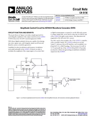
Circuit Note CN 0156 Circuits from the Lab™ reference circuits are engineered andtested for quick and easy system integration to help solve today’s analog, mixedignal, and RF design challenges. For more information and/or support visit www.analog.com/CN0281DevicesConnected/Referenced AD983475 MHz Complete Low Power DDS AD5620Bit Voltage Output nanoDAC® Amplitude Control Circuit for AD9834 Waveform Generator (DDS) Rev. A Circuits from the Lab™ circuits from Analog Devices have been designed and built by Analog Devices engineers. Standard engineering practices have been employed in the design and construction of each circuit, and their function and performance have been tested and verified in a lab environment at room temperature. H owever, you are solely responsible for testing the circuit and determining its suitability and applicability for your use and application. Accordingly, in no event shall Analog Devices be liable for direct, indirect, special, incidental, consequential or punitive damages due to any cause whatsoever connected to the use of any Circuits from the Lab circuits. (Continued on last page) One Technology Way, P.O. Box 9106, Norwood, MA 020629106, U.S.A.Tel: 781.329.4700www.analog.com Fax: 781.461.3113 © 2010 – 2013 Analog Devices, Inc. All rights reserved. CIRCUIT FUNCTION ANDBENEFITS AD5620GNDVDDVFBSYNCSCLKDINVOUTFS ADJUSTIOUTIOUTBFSYNCSCLKMCLKDGNDAGNDAD9834+3.3V+3.3V+3.3V MICRO SDATA AVDDDVDD = 6.8kΩ ADJUST PEAK-TO-PEAKUSING AD5620 09019-001 Figure . Low Power Amplitude Control Circuit for AD9834DDS (Simplified Schematic: All Connections and Decoupling Not Shown) Circuit Note ��Rev. | Page of CIRCUIT DESCRIPTIONThe circuit operates on a V to 5 V single supply. Both the DAC and DDS operate with an SPI interface. The onchipDAC for many DDS devices provides a complementary current output, IOUT and IOUTBfor the AD9834DDS.The reference current to the DAC is a function of theinternalreference voltage,REF, and an external resistor,SETwhich normally connectsfrom the DACFS ADJUST pinto ground. The reference current is equal to REFSEThere REFis the internal reference of the AD9834and has a typical value of 1.20TheSETresistor has a typical value of 6.8k.The fullscale current from the DAC is a multiple of the reference currentFor example, the fullscale current of theAD9834 SETFULLSCALE If FS ADJUST is connected to avarying voltage, DAC, the fullscale current is SETFULLSCALE Varying DACvaries the fullscale current and, therefore, the voltage output from the DDS device.You can provide thisvarying voltage by using a voltageoutput DAC.The AD5620is a low power, small, price effective solution here. A member of the nanoDAC family, it contains an chip 5 ppm/°C reference and is available in an 8leadSOT23 or MSOP package.The output voltage of the AD5620+2.The maximum fullscale output current is reached when DAC= 0 V (zeroscale) and the current from the AD9834swings between approximately 0.16 mA and 3.12 mA. With the loadresistor,the AD9834output voltage swings between approximately 0.032 V and 0.624 V. The output voltage on the IOUT pin of the AD98is shown in Figure where the DDS output frequency is set for 1 MHz. 09019-002 Figure DDS utput When Amplitude Control DAC Is Set to0 V(This Produces Maximum DDS FullScale Output)Increasing the voltage output from the AD5620reduces the fullscale output current of the AD9834. The minimum fullscale current will be reached when the voltage from the AD5620is equal to REF, or 1.20 V. Figure shows the AD9834output voltage for a halfscaloutput current, where VDAC= 0.REF, or 0.V. 09019-003 Figure DDS utputhen Amplitude Control DAC Is Set to0.(This Produces OneHalfScale DDS Output)The circuitmust be constructed on a multilayer PC board with a large area ground plane. Proper layout, grounding, and decoupling techniques must be used to achieve optimum performance (see 031 Tutorialand1 TutorialOMMON VARIATIONSThe AD5640and AD5660are 14bit and 16bit versionsrespectively,of the AD5620that aresuitable where higher resolutions are required. The AD9833offers the samefunctionalityof the AD9834without the amplitude modulation capability.LEARN MOREADIsimDDS Design and Evaluation ToolKester, Walt. The Data Conversion Handbook2005. Chapters 3, 7, and 8. Analog Devices.015 Tutorial, Basic DAC Architectures II: Binary DACsAnalog Devices.031 Tutorial, Grounding Data Converters and Solving the Mystery of AGND and DGND. Analog Devices.085 Tutorial, Fundamentals of Direct Digital Synthesis (DDS)Analog Devices101 Tutorial, Decoupling Techniques. Analog Devices.Riordan, Liam. 1070 Application Note, Programming the AD9833/AD9834Analog Devices Circuit Note ��Rev. | Page of Data Sheetsand Evaluation BoardsAD9834 Data SheetAD9834 Evaluation BoardAD5620 Data SheetAD5620 Evaluation BoardREVISION HISTORY7/13Rev. 0 to Rev. AChanges to Circuit Description Section and Figure 3 Caption/10Revision 0: Initial Version (Cont inued from first page) Circuits from the Lab circuits are intended only for use with Analog Devices products and are the intellectual property of An alog Devices or its licensors. While you may use the Circuits from the Lab circuits in the design of your pr oduct, no other license is granted by implication or otherwise under any patents or other intellectual property by application or use of the Circuits from the Lab circuits. Information furnished by Analog Devices is believed to be accurate and reliable. However, Circuits from the Lab circuits are supplied "as is" and without warranties of any kind, express, implied, or statutory including, but not limited to, any implied warranty of merchantability, noninfringement or fitness for a particular purpose and noresponsibility is assumed by Analog Devices for their use, nor for any infringements of patents or other rights of third parties that may result from their use. Analog Devices reserves the right to change any Circuits from the Lab circuits at any time wit hout notice but is under no obligation to do so. 20102013Analog Devices, Inc. All rights reserved. Trademarks and registered trademarks are the property of their respective owners. CN090197/13(A)