PDF-FlybackApplication Note AN-16stability, etc. This presents an enorm
June 1996
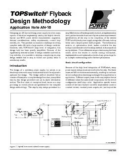
CM
CHOKEVACCX
VB
TOPSwitch
Output Capacitor
Output Post Filter L C
Bias CapacitorControl Pin Capacitor and Series Resistor
SOURCECONTROL
A
1 System Requirements
VACMIN
Download Presentation
"FlybackApplication Note AN-16stability, etc. This presents " is the property of its rightful owner. Permission is granted to download and print materials on this website for personal, non-commercial use only, provided you retain all copyright notices. By downloading content from our website, you accept the terms of this agreement.
Presentation Transcript
Transcript not available.