
ANALOG CIRCUITS A. A. Lande, E & TC Dept Course
PC
Published · 96 slides · 0 views
1 / 1


Description
ANALOG CIRCUITS A. A. Lande, E TC Dept Course outcome C302.3: Apply various applications of IC 741, IC 555 and oscillator for wave shaping. A. A. Lande, E TC Dept Operational Amplifier A. A. Lande, E TC Dept Introduction Various
Related Topics
Share
Embed code
Download this presentation From Below
"ANALOG CIRCUITS A. A. Lande, E & TC Dept Course" is the property of its rightful owner. Permission is granted to download and print the materials on this website for personal, non-commercial use only, and to display it on your personal computer provided you do not modify the materials and that you retain all copyright notices contained in the materials. By downloading content from our website, you accept the terms of this agreement.
Presentation Transcript
01
ANALOG CIRCUITS A. A. Lande, E & TC Dept<br>
02
Course outcome C302.3:
Apply various applications of IC 741, IC 555 and oscillator for wave shaping. A. A. Lande, E & TC Dept<br>
Apply various applications of IC 741, IC 555 and oscillator for wave shaping. A. A. Lande, E & TC Dept<br>
03
Operational Amplifier A. A. Lande, E & TC Dept<br>
04
Introduction Various branches of electronics are: Industrial electronics, Instrumentation, Communication, Power electronics etc.
Various electronic circuits used in the applications of these branches are amplifiers, waveform generators, timers, various arithmetic circuits such as adder, subtractor, multipliers, Log-antilog amplifier etc.
One electronic device which can be used to construct all the circuits mentioned above is called an operational amplifier or OP-AMP. A. A. Lande, E & TC Dept<br>
Various electronic circuits used in the applications of these branches are amplifiers, waveform generators, timers, various arithmetic circuits such as adder, subtractor, multipliers, Log-antilog amplifier etc.
One electronic device which can be used to construct all the circuits mentioned above is called an operational amplifier or OP-AMP. A. A. Lande, E & TC Dept<br>
05
OP-AMP Voltage amplifier using a transistor uses many other components such as coupling and bypass capacitors, biasing resistors etc.
In order to get higher voltage gain, we have to use more than one such amplifiers together. This will make the circuit bulky.
So people started using the amplifier in the integrated circuit (IC) form. A. A. Lande, E & TC Dept<br>
In order to get higher voltage gain, we have to use more than one such amplifiers together. This will make the circuit bulky.
So people started using the amplifier in the integrated circuit (IC) form. A. A. Lande, E & TC Dept<br>
06
Why it is called Operational Amplifier?
An OP-AMP is basically an amplifier which could be configured to perform a variety of operations such as amplification, addition, subtraction, differentiation and integration. Hence it is called operational amplifier.
OP-AMP is basically a multistage amplifier which uses a number of amplifier stages interconnected to each other in a complicated manner. A. A. Lande, E & TC Dept<br>
An OP-AMP is basically an amplifier which could be configured to perform a variety of operations such as amplification, addition, subtraction, differentiation and integration. Hence it is called operational amplifier.
OP-AMP is basically a multistage amplifier which uses a number of amplifier stages interconnected to each other in a complicated manner. A. A. Lande, E & TC Dept<br>
07
Advantages of OP-AMP over conventional amplifier:
It has smaller size.
Its reliability is higher than conventional amplifier.
Reduced cost.
Less power consumption.
Easy to replace.
Same OP-AMP can be used for various applications. A. A. Lande, E & TC Dept<br>
It has smaller size.
Its reliability is higher than conventional amplifier.
Reduced cost.
Less power consumption.
Easy to replace.
Same OP-AMP can be used for various applications. A. A. Lande, E & TC Dept<br>
08
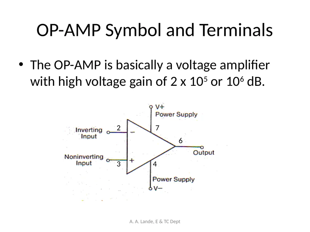
OP-AMP Symbol and Terminals The OP-AMP is basically a voltage amplifier with high voltage gain of 2 x 10⁵ or 106 dB. 2 3 7 4 6 A. A. Lande, E & TC Dept<br>
09
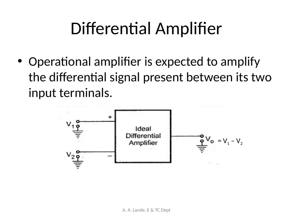
Differential Amplifier Operational amplifier is expected to amplify the differential signal present between its two input terminals. = V1 – V2 A. A. Lande, E & TC Dept<br>
10
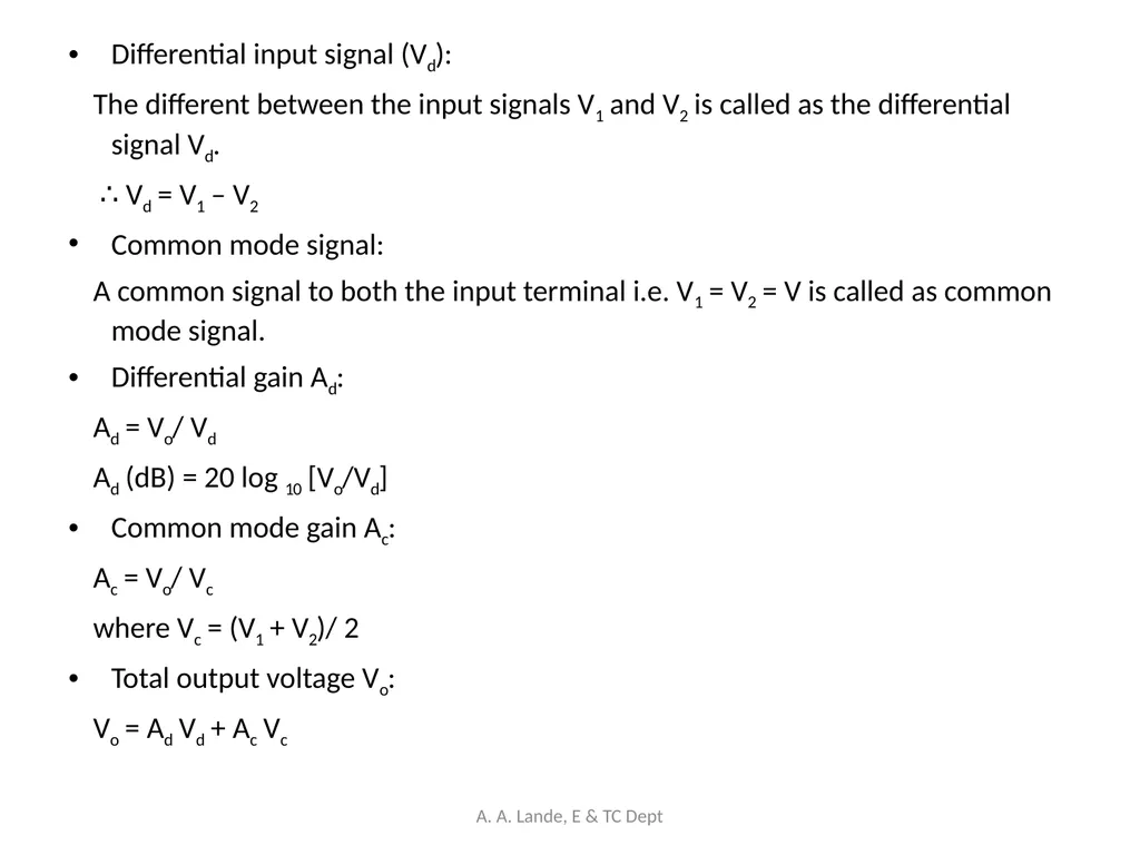
Differential input signal (Vd):
The different between the input signals V1 and V2 is called as the differential signal Vd.
∴ Vd = V1 – V2
Common mode signal:
A common signal to both the input terminal i.e. V1 = V2 = V is called as common mode signal.
Differential gain Ad:
Ad = Vo/ Vd
Ad (dB) = 20 log 10 [Vo/Vd]
Common mode gain Ac:
Ac = Vo/ Vc
where Vc = (V1 + V2)/ 2
Total output voltage Vo:
Vo = Ad Vd + Ac Vc A. A. Lande, E & TC Dept<br>
The different between the input signals V1 and V2 is called as the differential signal Vd.
∴ Vd = V1 – V2
Common mode signal:
A common signal to both the input terminal i.e. V1 = V2 = V is called as common mode signal.
Differential gain Ad:
Ad = Vo/ Vd
Ad (dB) = 20 log 10 [Vo/Vd]
Common mode gain Ac:
Ac = Vo/ Vc
where Vc = (V1 + V2)/ 2
Total output voltage Vo:
Vo = Ad Vd + Ac Vc A. A. Lande, E & TC Dept<br>
11
Common Mode Rejection ratio (CMRR):
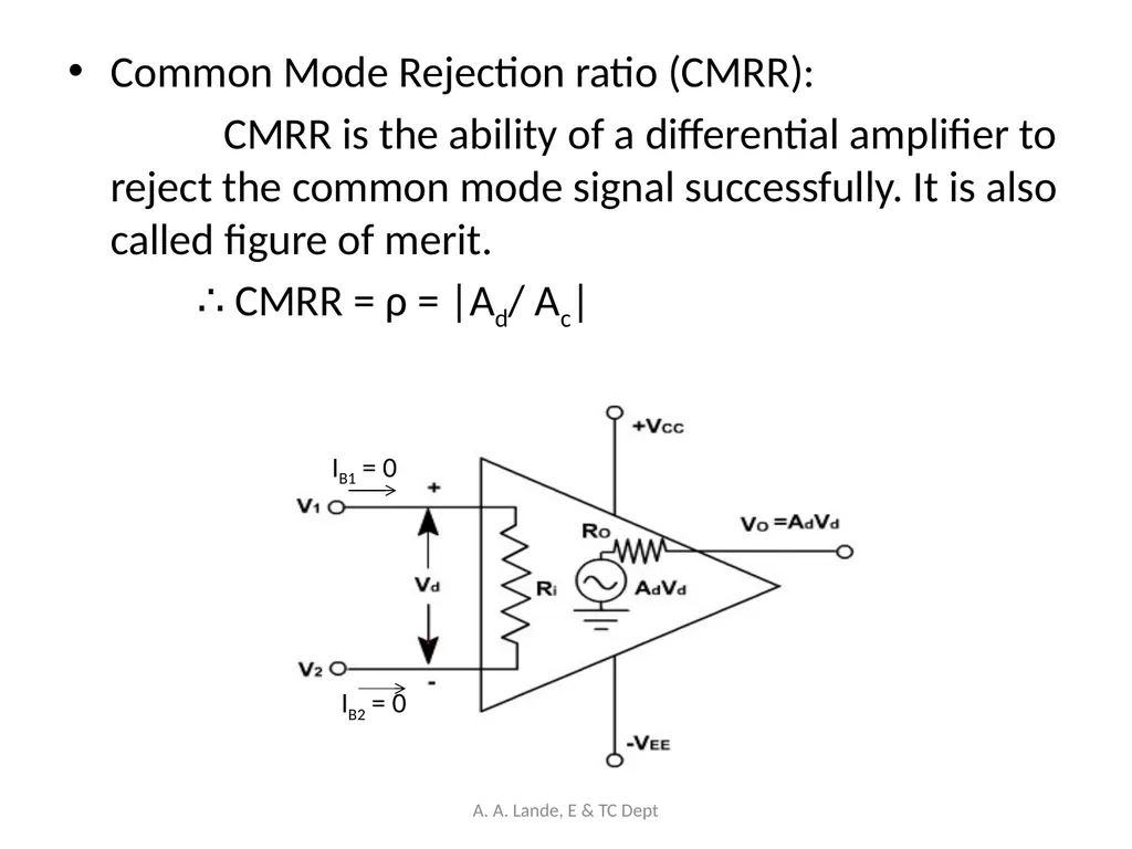
CMRR is the ability of a differential amplifier to reject the common mode signal successfully. It is also called figure of merit.
∴ CMRR = ρ = |Ad/ Ac| IB1 = 0 IB2 = 0 A. A. Lande, E & TC Dept<br>
CMRR is the ability of a differential amplifier to reject the common mode signal successfully. It is also called figure of merit.
∴ CMRR = ρ = |Ad/ Ac| IB1 = 0 IB2 = 0 A. A. Lande, E & TC Dept<br>
12
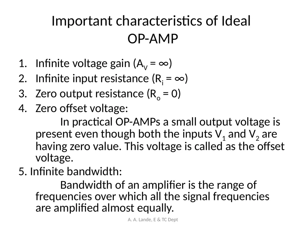
Important characteristics of Ideal
OP-AMP Infinite voltage gain (AV = ∞)
Infinite input resistance (Ri = ∞)
Zero output resistance (Ro = 0)
Zero offset voltage:
In practical OP-AMPs a small output voltage is present even though both the inputs V1 and V2 are having zero value. This voltage is called as the offset voltage.
5. Infinite bandwidth:
Bandwidth of an amplifier is the range of frequencies over which all the signal frequencies are amplified almost equally. A. A. Lande, E & TC Dept<br>
Infinite input resistance (Ri = ∞)
Zero output resistance (Ro = 0)
Zero offset voltage:
In practical OP-AMPs a small output voltage is present even though both the inputs V1 and V2 are having zero value. This voltage is called as the offset voltage.
5. Infinite bandwidth:
Bandwidth of an amplifier is the range of frequencies over which all the signal frequencies are amplified almost equally. A. A. Lande, E & TC Dept<br>
13
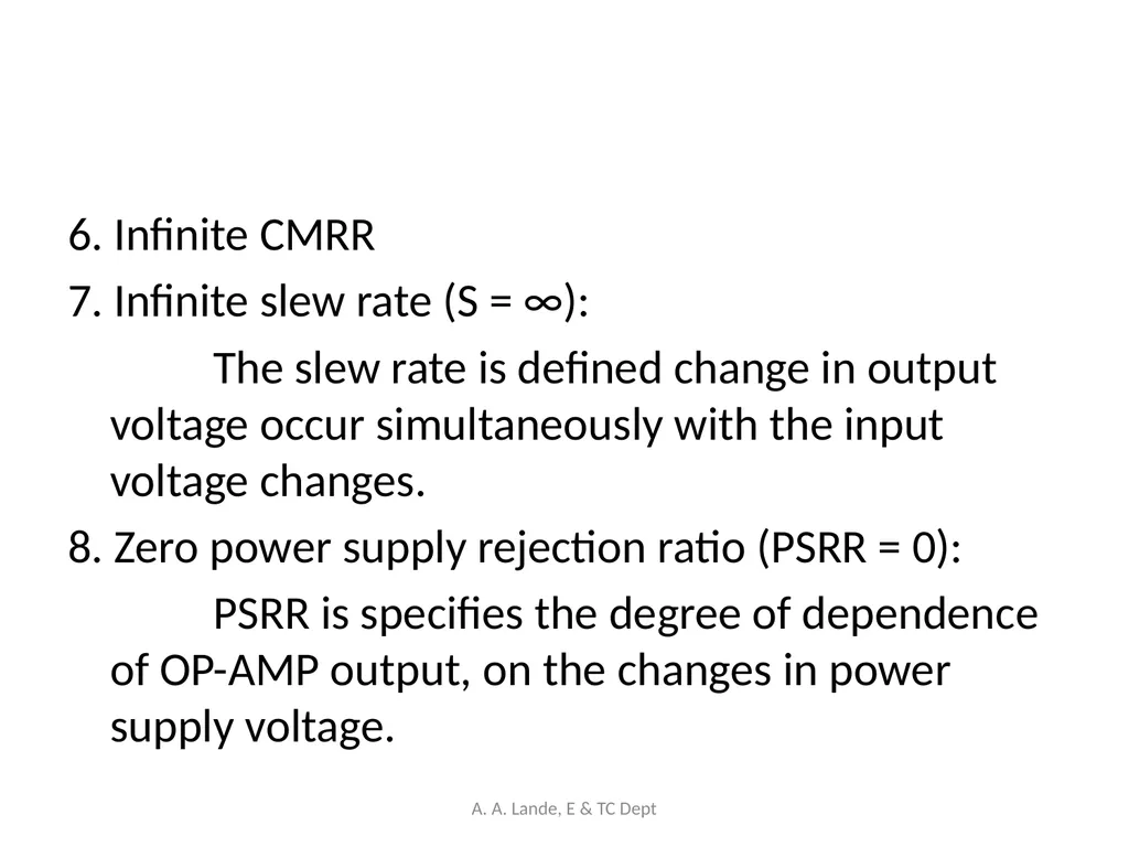
6. Infinite CMRR
7. Infinite slew rate (S = ∞):
The slew rate is defined change in output voltage occur simultaneously with the input voltage changes.
8. Zero power supply rejection ratio (PSRR = 0):
PSRR is specifies the degree of dependence of OP-AMP output, on the changes in power supply voltage. A. A. Lande, E & TC Dept<br>
7. Infinite slew rate (S = ∞):
The slew rate is defined change in output voltage occur simultaneously with the input voltage changes.
8. Zero power supply rejection ratio (PSRR = 0):
PSRR is specifies the degree of dependence of OP-AMP output, on the changes in power supply voltage. A. A. Lande, E & TC Dept<br>
14
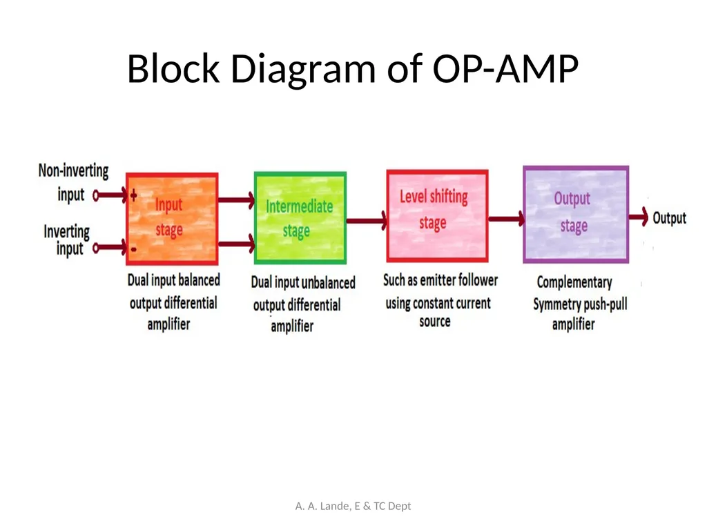
Block Diagram of OP-AMP A. A. Lande, E & TC Dept<br>
15
The Op-AMP consists of:
Input stage
Intermediate stage
Level shifting stage
Output stage
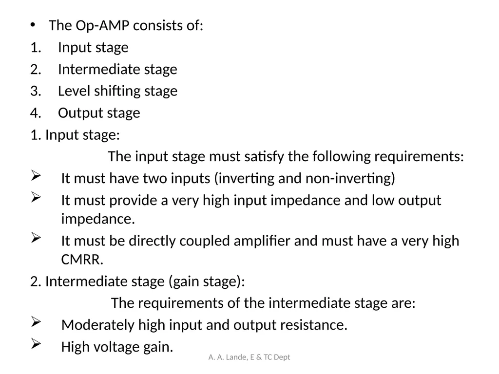
1. Input stage:
The input stage must satisfy the following requirements:
It must have two inputs (inverting and non-inverting)
It must provide a very high input impedance and low output impedance.
It must be directly coupled amplifier and must have a very high CMRR.
2. Intermediate stage (gain stage):
The requirements of the intermediate stage are:
Moderately high input and output resistance.
High voltage gain. A. A. Lande, E & TC Dept<br>
Input stage
Intermediate stage
Level shifting stage
Output stage
1. Input stage:
The input stage must satisfy the following requirements:
It must have two inputs (inverting and non-inverting)
It must provide a very high input impedance and low output impedance.
It must be directly coupled amplifier and must have a very high CMRR.
2. Intermediate stage (gain stage):
The requirements of the intermediate stage are:
Moderately high input and output resistance.
High voltage gain. A. A. Lande, E & TC Dept<br>
16
3. Level shifting stage:
Due to the direct coupling between the first two stages, the input of level shifting stage is an amplified signal with some nonzero dc level.
Level shifting stage is used to bring this dc level to zero volts with respect to ground.
4. Output stage:
Requirements of output stage:
Low output resistance
Large current sourcing capacity.
Large output voltage swing. A. A. Lande, E & TC Dept<br>
Due to the direct coupling between the first two stages, the input of level shifting stage is an amplified signal with some nonzero dc level.
Level shifting stage is used to bring this dc level to zero volts with respect to ground.
4. Output stage:
Requirements of output stage:
Low output resistance
Large current sourcing capacity.
Large output voltage swing. A. A. Lande, E & TC Dept<br>
17
OP-AMP IC 741 This is one of the oldest and most popular OP-AMP IC.
Features of IC 741:
No frequency compensation required.
Short circuit protection.
Offset voltage null capability.
Large common mode and differential voltage ranges.
No latch ups. A. A. Lande, E & TC Dept<br>
Features of IC 741:
No frequency compensation required.
Short circuit protection.
Offset voltage null capability.
Large common mode and differential voltage ranges.
No latch ups. A. A. Lande, E & TC Dept<br>
18
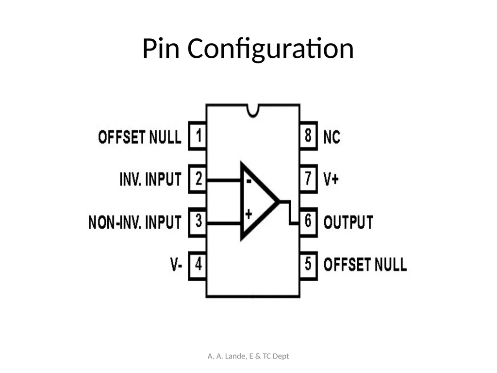
Pin Configuration A. A. Lande, E & TC Dept<br>
19
Pin configuration:
IC 741 is 8 pin IC.
Pin 1 and 5:
These pins can be used to nullify the offset voltage.
Pin 2 and 3:
Pin number 2 and 3 are inverting and non-inverting inputs respectively.
Pin 4 and 7:
Pin number 7 is for connecting the positive supply voltage +VCC while pin number 4 is to be connected to a negative supply voltage. Thus IC 741 needs a dual polarity power supply.
Pin 6:
We get the output voltage at pin number 6.
Pin 8:
Pin number 8 is a dummy pin which is not connected anywhere and hence should be left open or unconnected. A. A. Lande, E & TC Dept<br>
IC 741 is 8 pin IC.
Pin 1 and 5:
These pins can be used to nullify the offset voltage.
Pin 2 and 3:
Pin number 2 and 3 are inverting and non-inverting inputs respectively.
Pin 4 and 7:
Pin number 7 is for connecting the positive supply voltage +VCC while pin number 4 is to be connected to a negative supply voltage. Thus IC 741 needs a dual polarity power supply.
Pin 6:
We get the output voltage at pin number 6.
Pin 8:
Pin number 8 is a dummy pin which is not connected anywhere and hence should be left open or unconnected. A. A. Lande, E & TC Dept<br>
20
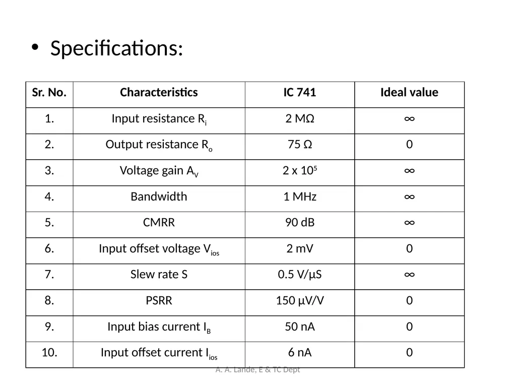
Specifications: A. A. Lande, E & TC Dept<br>
21
Applications:
Inverting and non inverting amplifiers.
Adder, subtractor.
Integrator, differentiator circuits.
Other applications such as V to I and I to V converter, precision rectifier, log, antilog amplifier etc. A. A. Lande, E & TC Dept<br>
Inverting and non inverting amplifiers.
Adder, subtractor.
Integrator, differentiator circuits.
Other applications such as V to I and I to V converter, precision rectifier, log, antilog amplifier etc. A. A. Lande, E & TC Dept<br>
22
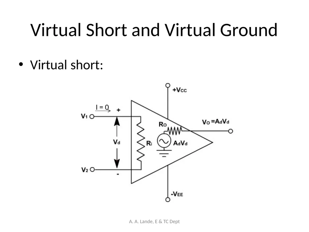
Virtual Short and Virtual Ground Virtual short: I = 0 A. A. Lande, E & TC Dept<br>
23
According to virtual short concept, both the input terminals are approximately at the same potential.
The output voltage of an OP-AMP is given by,
Vo = AV x Vd
where, AV = open loop gain and
Vd = Differential input voltage
∴ Vd = VO / AV
but AV = ∞ for an ideal op-amp and AV = 2 x 10⁵ for IC 741.
∴ for ideal op-amp, Vd = 0. Thus the potential difference between the input terminals is zero. A. A. Lande, E & TC Dept<br>
The output voltage of an OP-AMP is given by,
Vo = AV x Vd
where, AV = open loop gain and
Vd = Differential input voltage
∴ Vd = VO / AV
but AV = ∞ for an ideal op-amp and AV = 2 x 10⁵ for IC 741.
∴ for ideal op-amp, Vd = 0. Thus the potential difference between the input terminals is zero. A. A. Lande, E & TC Dept<br>
24
Virtual ground:
If the non-inverting terminal of OP-AMP is connected to ground, then due to the “virtual short” existing between the two input terminals, the inverting terminal will also be at ground potential.
Hence it is said to be at “virtual ground.” A. A. Lande, E & TC Dept<br>
If the non-inverting terminal of OP-AMP is connected to ground, then due to the “virtual short” existing between the two input terminals, the inverting terminal will also be at ground potential.
Hence it is said to be at “virtual ground.” A. A. Lande, E & TC Dept<br>
25
Configurations of OP-AMP An op-amp can work in two different modes:
Open loop mode 2. closed loop mode
Open loop configuration:
The open loop configuration is that there is absolutely no feedback present from the output to input. A. A. Lande, E & TC Dept<br>
Open loop mode 2. closed loop mode
Open loop configuration:
The open loop configuration is that there is absolutely no feedback present from the output to input. A. A. Lande, E & TC Dept<br>
26
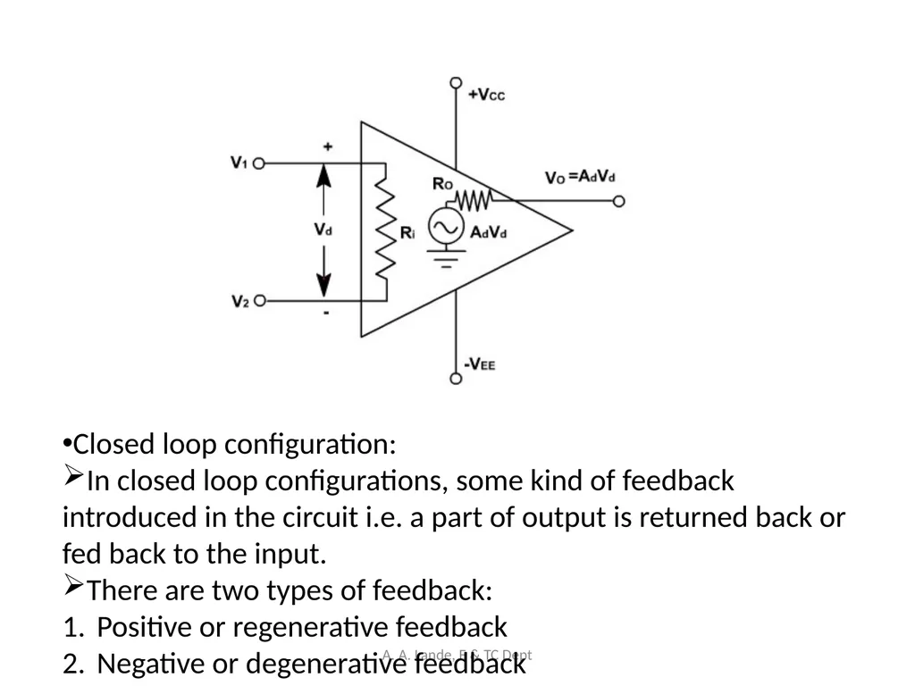
Closed loop configuration:
In closed loop configurations, some kind of feedback introduced in the circuit i.e. a part of output is returned back or fed back to the input.
There are two types of feedback:
Positive or regenerative feedback
Negative or degenerative feedback A. A. Lande, E & TC Dept<br>
In closed loop configurations, some kind of feedback introduced in the circuit i.e. a part of output is returned back or fed back to the input.
There are two types of feedback:
Positive or regenerative feedback
Negative or degenerative feedback A. A. Lande, E & TC Dept<br>
27
Positive feedback:
If the feedback signal or original signal are in phase with each other then it is called as the positive feed back.
This feedback used in applications such as “oscillator” and Schmitt trigger.
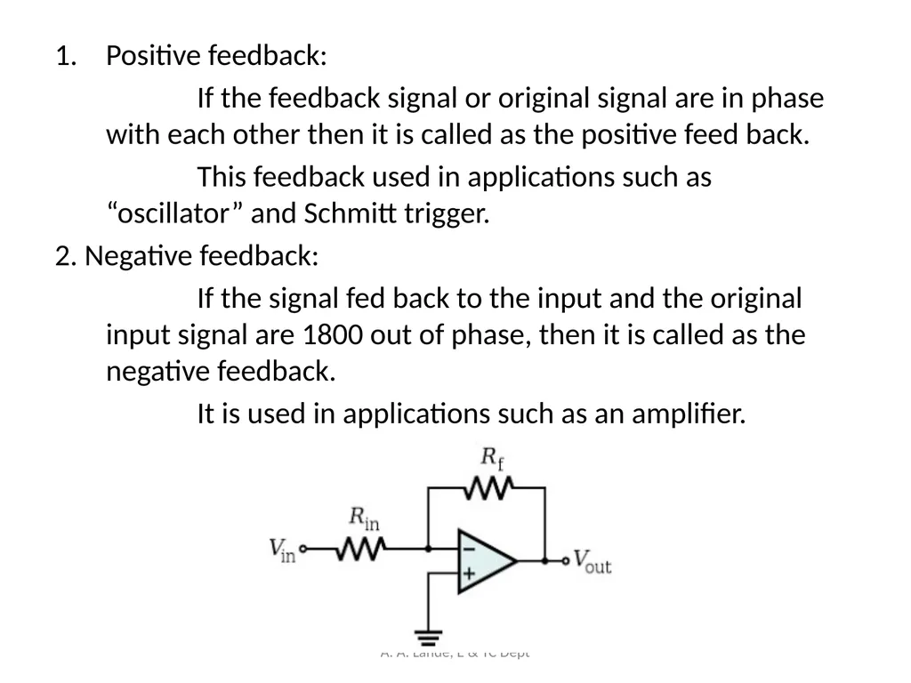
2. Negative feedback:
If the signal fed back to the input and the original input signal are 1800 out of phase, then it is called as the negative feedback.
It is used in applications such as an amplifier. A. A. Lande, E & TC Dept<br>
If the feedback signal or original signal are in phase with each other then it is called as the positive feed back.
This feedback used in applications such as “oscillator” and Schmitt trigger.
2. Negative feedback:
If the signal fed back to the input and the original input signal are 1800 out of phase, then it is called as the negative feedback.
It is used in applications such as an amplifier. A. A. Lande, E & TC Dept<br>
28
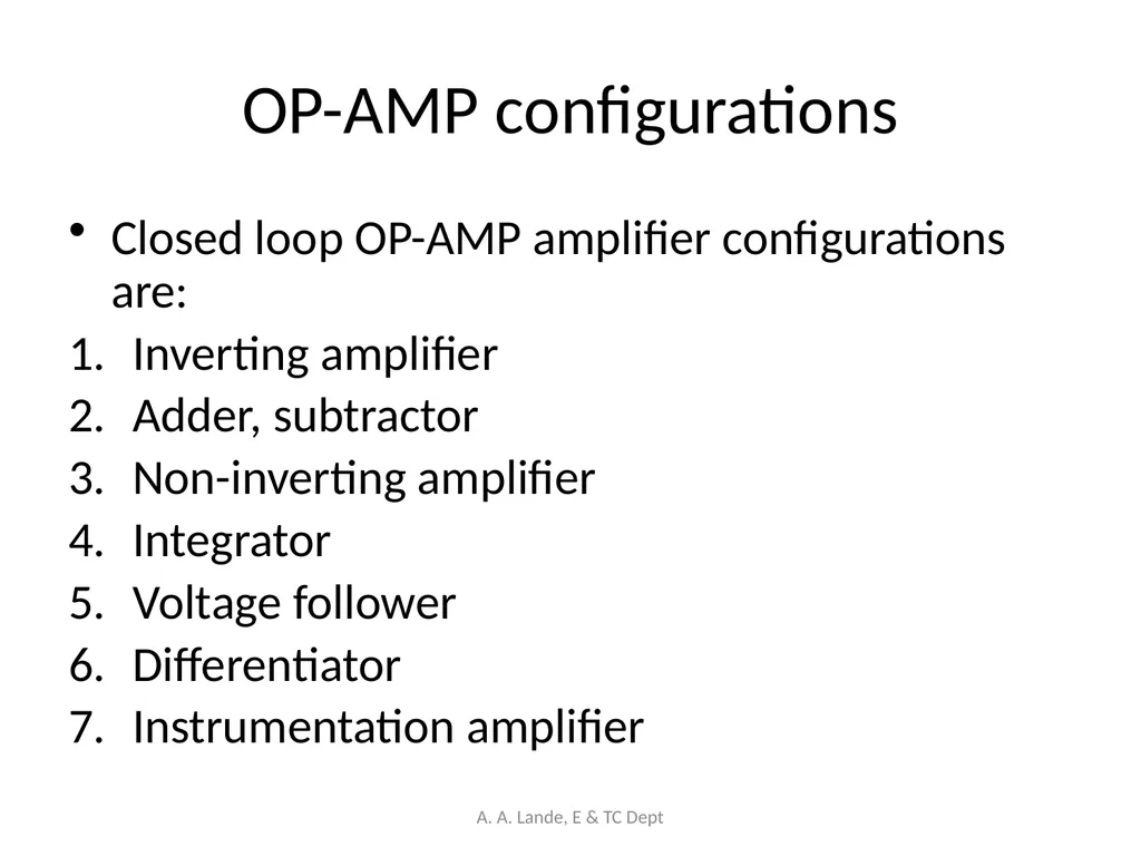
OP-AMP configurations Closed loop OP-AMP amplifier configurations are:
Inverting amplifier
Adder, subtractor
Non-inverting amplifier
Integrator
Voltage follower
Differentiator
Instrumentation amplifier A. A. Lande, E & TC Dept<br>
Inverting amplifier
Adder, subtractor
Non-inverting amplifier
Integrator
Voltage follower
Differentiator
Instrumentation amplifier A. A. Lande, E & TC Dept<br>
29
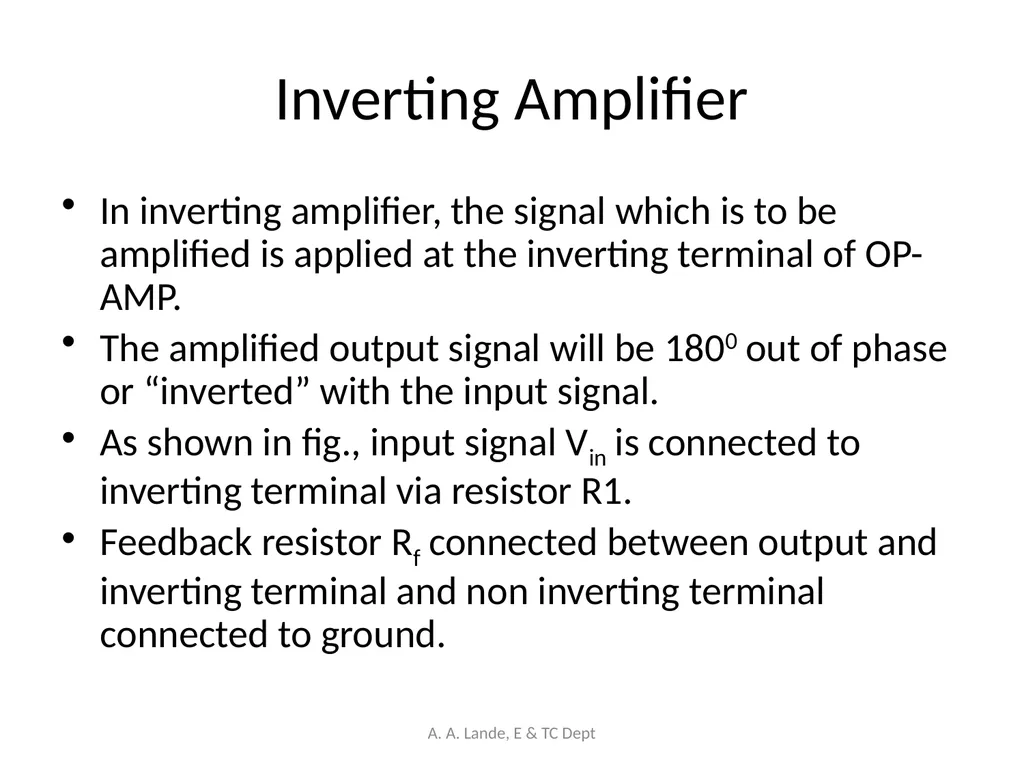
Inverting Amplifier In inverting amplifier, the signal which is to be amplified is applied at the inverting terminal of OP-AMP.
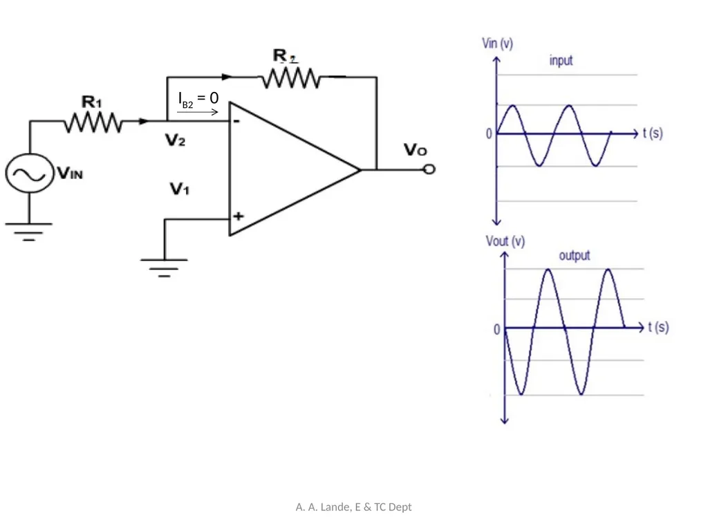
The amplified output signal will be 1800 out of phase or “inverted” with the input signal.
As shown in fig., input signal Vin is connected to inverting terminal via resistor R1.
Feedback resistor Rf connected between output and inverting terminal and non inverting terminal connected to ground. A. A. Lande, E & TC Dept<br>
The amplified output signal will be 1800 out of phase or “inverted” with the input signal.
As shown in fig., input signal Vin is connected to inverting terminal via resistor R1.
Feedback resistor Rf connected between output and inverting terminal and non inverting terminal connected to ground. A. A. Lande, E & TC Dept<br>
30
IB2 = 0 A. A. Lande, E & TC Dept<br>
31
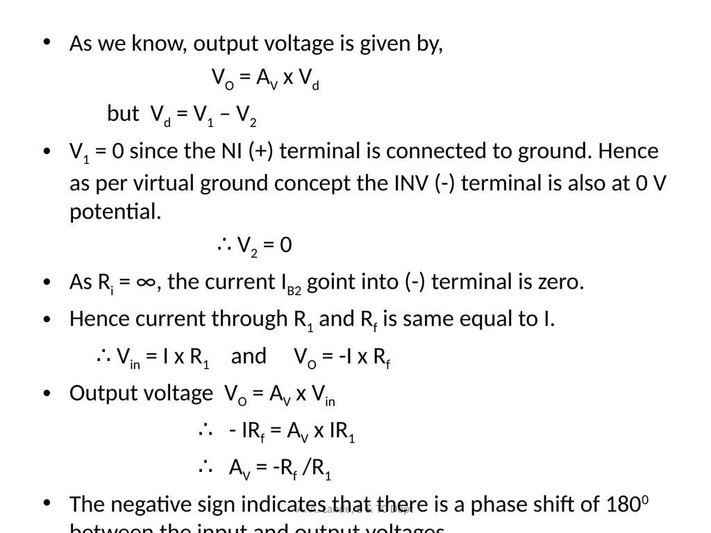
As we know, output voltage is given by,
VO = AV x Vd
but Vd = V1 – V2
V1 = 0 since the NI (+) terminal is connected to ground. Hence as per virtual ground concept the INV (-) terminal is also at 0 V potential.
∴ V2 = 0
As Ri = ∞, the current IB2 goint into (-) terminal is zero.
Hence current through R1 and Rf is same equal to I.
∴ Vin = I x R1 and VO = -I x Rf
Output voltage VO = AV x Vin
∴ - IRf = AV x IR1
∴ AV = -Rf /R1
The negative sign indicates that there is a phase shift of 1800 between the input and output voltages A. A. Lande, E & TC Dept<br>
VO = AV x Vd
but Vd = V1 – V2
V1 = 0 since the NI (+) terminal is connected to ground. Hence as per virtual ground concept the INV (-) terminal is also at 0 V potential.
∴ V2 = 0
As Ri = ∞, the current IB2 goint into (-) terminal is zero.
Hence current through R1 and Rf is same equal to I.
∴ Vin = I x R1 and VO = -I x Rf
Output voltage VO = AV x Vin
∴ - IRf = AV x IR1
∴ AV = -Rf /R1
The negative sign indicates that there is a phase shift of 1800 between the input and output voltages A. A. Lande, E & TC Dept<br>
32
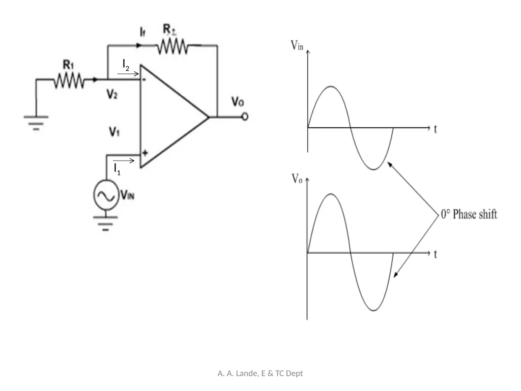
Non- Inverting Amplifier In non-inverting amplifier, input signal is applied to the non-inverting (+) terminal.
Feedback resistor Rf is connected between output and inverting terminal.
Input and output voltages are in phase with each other.
For ideal Op-AMP, Ri = ∞, therefore the currents entering into both the input terminals of opamp will be zero. (I1 = I2 = 0) A. A. Lande, E & TC Dept<br>
Feedback resistor Rf is connected between output and inverting terminal.
Input and output voltages are in phase with each other.
For ideal Op-AMP, Ri = ∞, therefore the currents entering into both the input terminals of opamp will be zero. (I1 = I2 = 0) A. A. Lande, E & TC Dept<br>
33
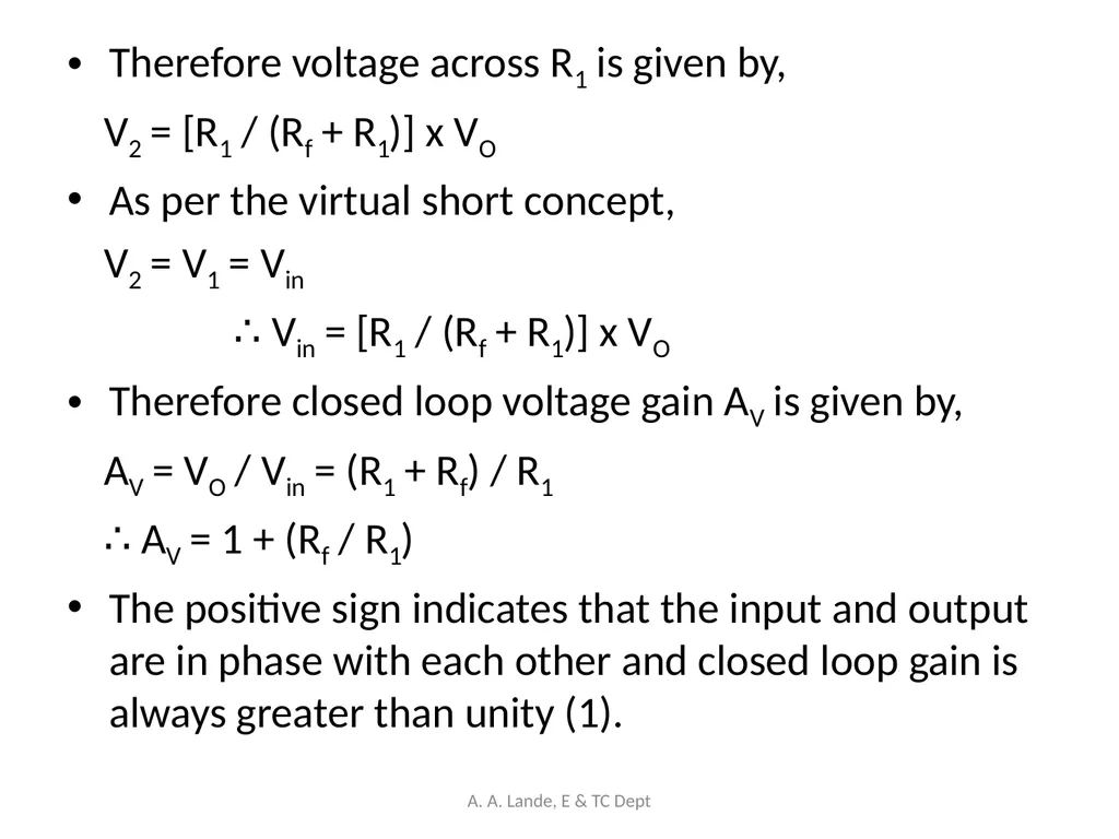
Therefore voltage across R1 is given by,
V2 = [R1 / (Rf + R1)] x VO
As per the virtual short concept,
V2 = V1 = Vin
∴ Vin = [R1 / (Rf + R1)] x VO
Therefore closed loop voltage gain AV is given by,
AV = VO / Vin = (R1 + Rf) / R1
∴ AV = 1 + (Rf / R1)
The positive sign indicates that the input and output are in phase with each other and closed loop gain is always greater than unity (1). A. A. Lande, E & TC Dept<br>
V2 = [R1 / (Rf + R1)] x VO
As per the virtual short concept,
V2 = V1 = Vin
∴ Vin = [R1 / (Rf + R1)] x VO
Therefore closed loop voltage gain AV is given by,
AV = VO / Vin = (R1 + Rf) / R1
∴ AV = 1 + (Rf / R1)
The positive sign indicates that the input and output are in phase with each other and closed loop gain is always greater than unity (1). A. A. Lande, E & TC Dept<br>
34
I2 I1 A. A. Lande, E & TC Dept<br>
35
Summing amplifier or Adder If more than one input signal is applied to an any one input terminal of OP-AMP, the circuit will add all these input signals to produce their addition at the output.
Adder circuit can be classified into two categories as:
Inverting adder
Non-inverting adder A. A. Lande, E & TC Dept<br>
Adder circuit can be classified into two categories as:
Inverting adder
Non-inverting adder A. A. Lande, E & TC Dept<br>
36
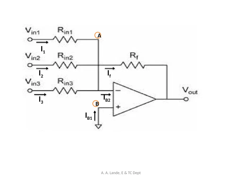
Inverting Adder Fig. shows the inverting summing amplifier with three inputs Vin1, Vin2 and Vin3 are applied to the inverting terminal through resistors Rin1, Rin2 and Rin3 respectively and Rf is the feedback resistor.
Expression for output voltage:
Let current through resistors Rin1, Rin2 and Rin3 be I1, I2 and I3 respectively.
apply KCL at node A to write,
I1 + I2 + I3 = IB2 + If ------(1) A. A. Lande, E & TC Dept<br>
Expression for output voltage:
Let current through resistors Rin1, Rin2 and Rin3 be I1, I2 and I3 respectively.
apply KCL at node A to write,
I1 + I2 + I3 = IB2 + If ------(1) A. A. Lande, E & TC Dept<br>
37
But for ideal op-amp, Ri = ∞, therefore IB2 = 0 and VA = VB = 0 due to virtual ground concept.
Hence, I1 + I2 + I3 = If
From input side, I1 = (V1 - VA) / Rin1 = V1 / Rin1
Similarly, I2 = (V2 - VA) / Rin2 = V2 / Rin2
and I3 = (V3 - VA) / Rin3 = V3 / Rin3
And from output side,
If = (VA – VO) / Rf = (- VO) / Rf
Substituting these values in eq. 1, we get,
(V1/ Rin1) + (V2/ Rin2) + (V3 / Rin3) = (-VO / Rf)
∴ VO = - [(Rf/Rin1)V1 + (Rf/Rin2)V2 + (Rf/Rin3)V3]
If we substitute Rf = Rin1 = Rin2 = Rin3 = R, then we get
VO = - (V1 + V2 + V3)
Thus output voltage is the negative sum of the input voltage. Therefore this circuit is called as “inverting adder”. A. A. Lande, E & TC Dept<br>
Hence, I1 + I2 + I3 = If
From input side, I1 = (V1 - VA) / Rin1 = V1 / Rin1
Similarly, I2 = (V2 - VA) / Rin2 = V2 / Rin2
and I3 = (V3 - VA) / Rin3 = V3 / Rin3
And from output side,
If = (VA – VO) / Rf = (- VO) / Rf
Substituting these values in eq. 1, we get,
(V1/ Rin1) + (V2/ Rin2) + (V3 / Rin3) = (-VO / Rf)
∴ VO = - [(Rf/Rin1)V1 + (Rf/Rin2)V2 + (Rf/Rin3)V3]
If we substitute Rf = Rin1 = Rin2 = Rin3 = R, then we get
VO = - (V1 + V2 + V3)
Thus output voltage is the negative sum of the input voltage. Therefore this circuit is called as “inverting adder”. A. A. Lande, E & TC Dept<br>
38
A B I1 I2 I3 If IB2 IB1 A. A. Lande, E & TC Dept<br>
39
Non - Inverting Adder An adder circuit which can produce the addition of its input signals without inversion is called as the non-inverting adder.
Fig. shows the non-inverting adder with two inputs V1 and V2.
The output voltage is given by,
VO = V1 + V2
The positive sign indicates that the inversion does not take place in this adder and therefore it is called as the non-inverting adder. A. A. Lande, E & TC Dept<br>
Fig. shows the non-inverting adder with two inputs V1 and V2.
The output voltage is given by,
VO = V1 + V2
The positive sign indicates that the inversion does not take place in this adder and therefore it is called as the non-inverting adder. A. A. Lande, E & TC Dept<br>
40
A. A. Lande, E & TC Dept<br>
41
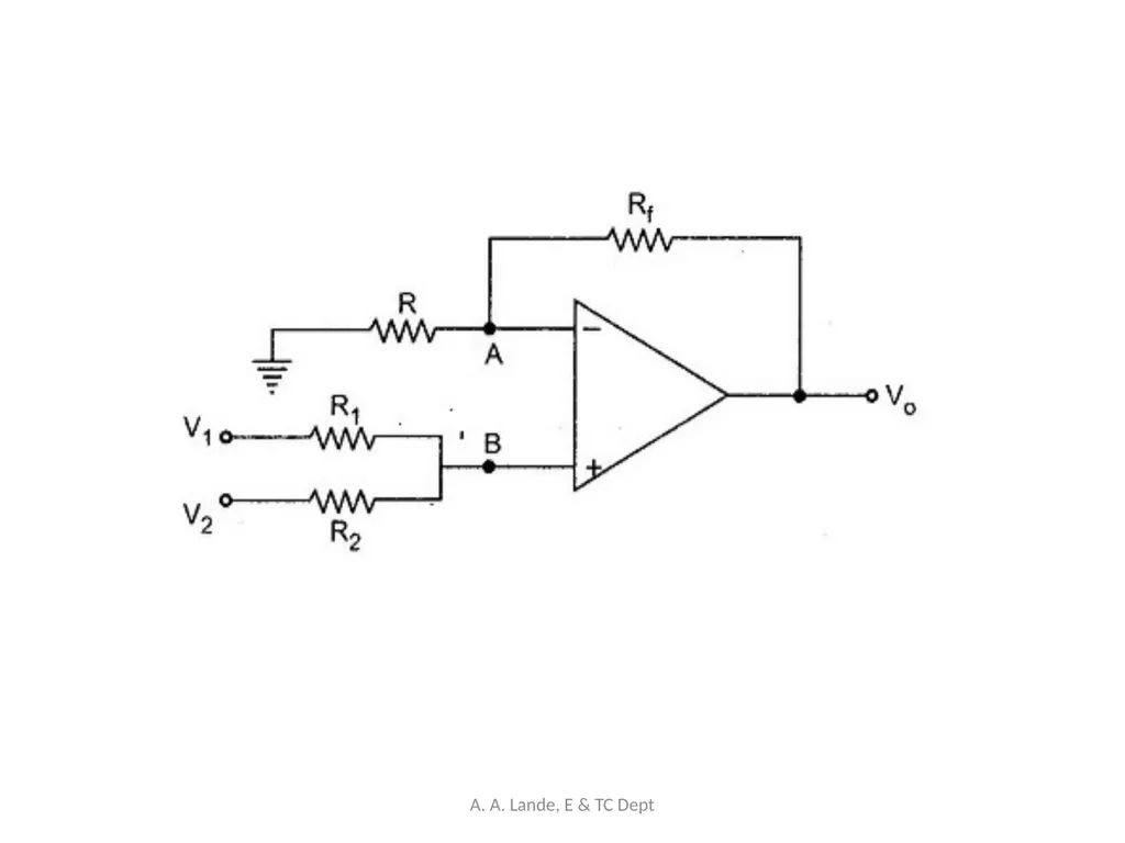
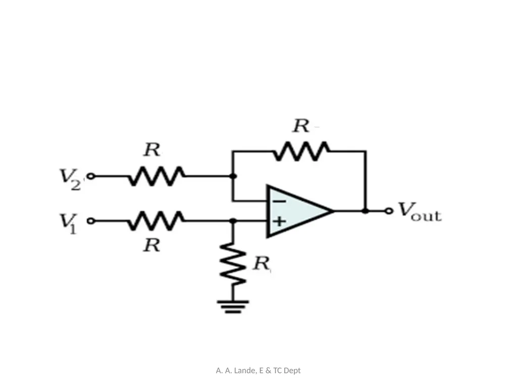
Difference Amplifier The difference amplifier and subtractor circuits are used to obtain the subtraction of two input voltages.
Fig. shows the difference amplifier.
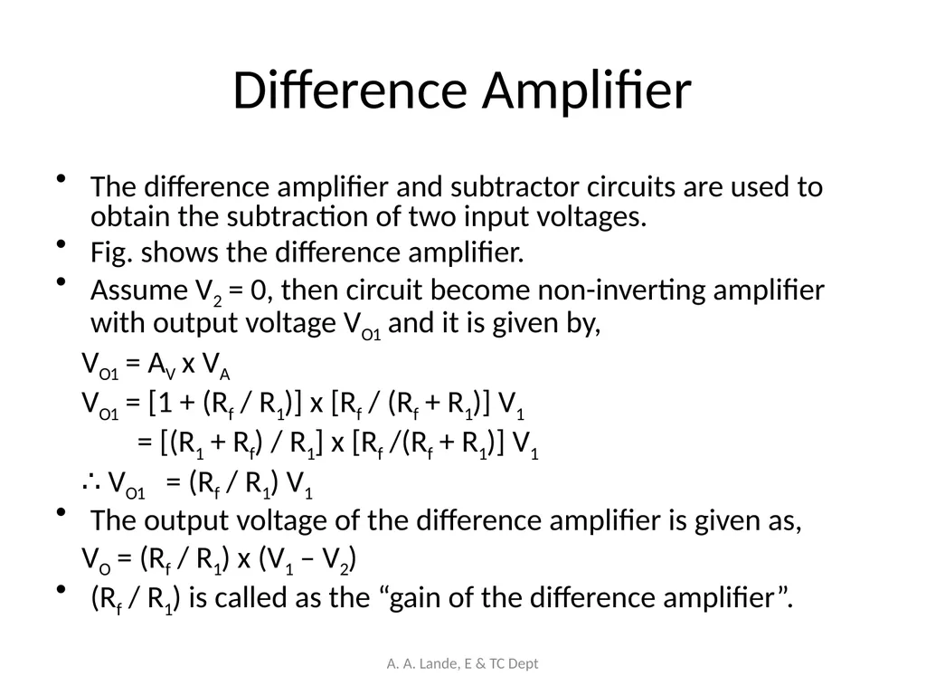
Assume V2 = 0, then circuit become non-inverting amplifier with output voltage VO1 and it is given by,
VO1 = AV x VA
VO1 = [1 + (Rf / R1)] x [Rf / (Rf + R1)] V1
= [(R1 + Rf) / R1] x [Rf /(Rf + R1)] V1
∴ VO1 = (Rf / R1) V1
The output voltage of the difference amplifier is given as,
VO = (Rf / R1) x (V1 – V2)
(Rf / R1) is called as the “gain of the difference amplifier”. A. A. Lande, E & TC Dept<br>
Fig. shows the difference amplifier.
Assume V2 = 0, then circuit become non-inverting amplifier with output voltage VO1 and it is given by,
VO1 = AV x VA
VO1 = [1 + (Rf / R1)] x [Rf / (Rf + R1)] V1
= [(R1 + Rf) / R1] x [Rf /(Rf + R1)] V1
∴ VO1 = (Rf / R1) V1
The output voltage of the difference amplifier is given as,
VO = (Rf / R1) x (V1 – V2)
(Rf / R1) is called as the “gain of the difference amplifier”. A. A. Lande, E & TC Dept<br>
42
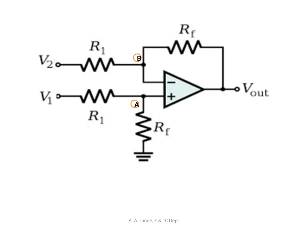
A B A. A. Lande, E & TC Dept<br>
43
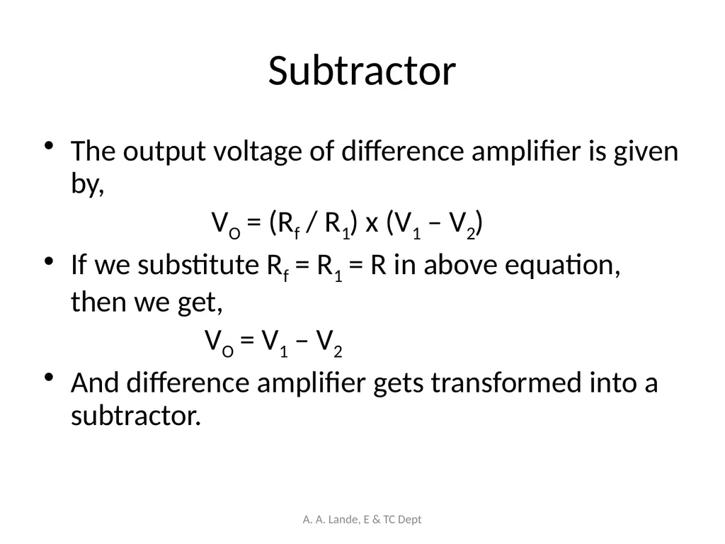
Subtractor The output voltage of difference amplifier is given by,
VO = (Rf / R1) x (V1 – V2)
If we substitute Rf = R1 = R in above equation, then we get,
VO = V1 – V2
And difference amplifier gets transformed into a subtractor. A. A. Lande, E & TC Dept<br>
VO = (Rf / R1) x (V1 – V2)
If we substitute Rf = R1 = R in above equation, then we get,
VO = V1 – V2
And difference amplifier gets transformed into a subtractor. A. A. Lande, E & TC Dept<br>
44
A. A. Lande, E & TC Dept<br>
45
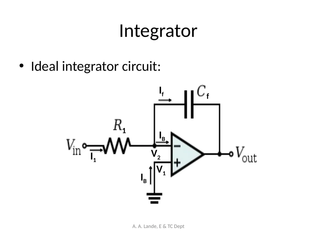
Integrator Ideal integrator circuit: I1 If IB V2 V1 IB 1 f A. A. Lande, E & TC Dept<br>
46
The ideal integrator circuit is obtained by replacing the feedback resistor Rf in the inverting amplifier configuration by “C”.
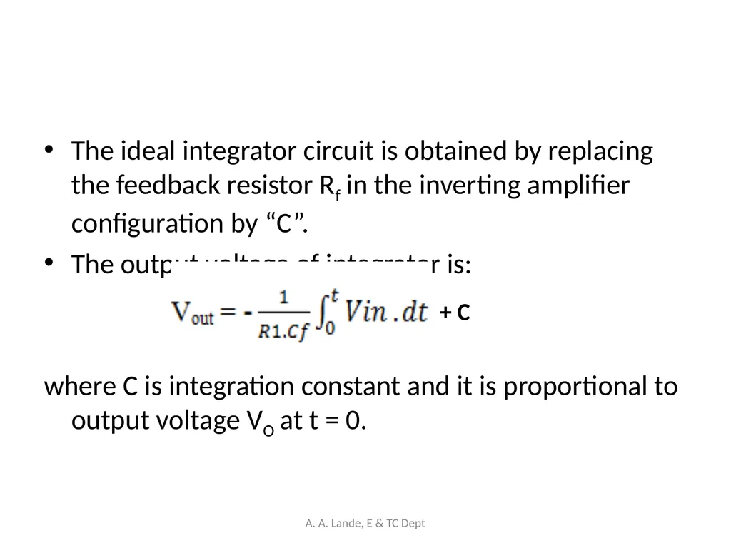
The output voltage of integrator is:
where C is integration constant and it is proportional to output voltage VO at t = 0. + C A. A. Lande, E & TC Dept<br>
The output voltage of integrator is:
where C is integration constant and it is proportional to output voltage VO at t = 0. + C A. A. Lande, E & TC Dept<br>
47
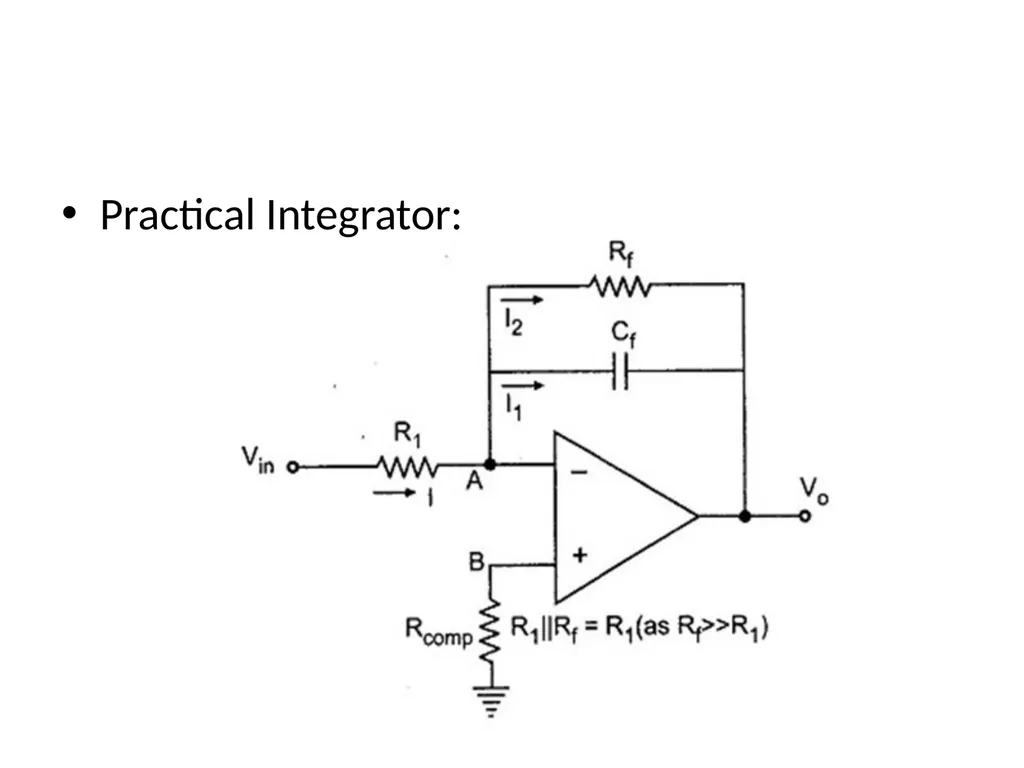
Practical Integrator: A. A. Lande, E & TC Dept<br>
48
Applications of an integrator:
In the triangular wave or ramp generator
In the analog to digital converter
In analog computers to solve differential equations.
As a low pass filter. A. A. Lande, E & TC Dept<br>
In the triangular wave or ramp generator
In the analog to digital converter
In analog computers to solve differential equations.
As a low pass filter. A. A. Lande, E & TC Dept<br>
49
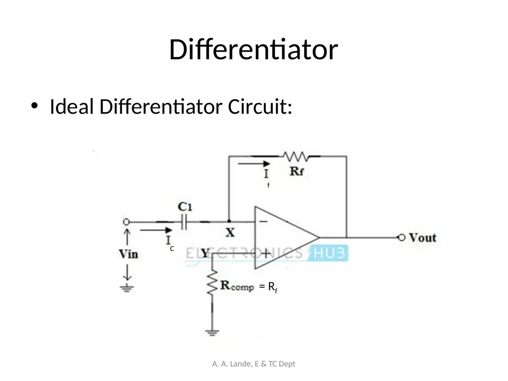
Differentiator Ideal Differentiator Circuit: C = Rf f A. A. Lande, E & TC Dept<br>
50
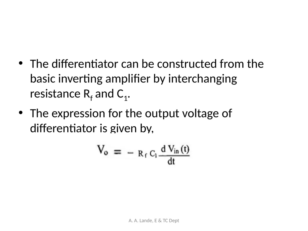
The differentiator can be constructed from the basic inverting amplifier by interchanging resistance Rf and C1.
The expression for the output voltage of differentiator is given by, A. A. Lande, E & TC Dept<br>
The expression for the output voltage of differentiator is given by, A. A. Lande, E & TC Dept<br>
51
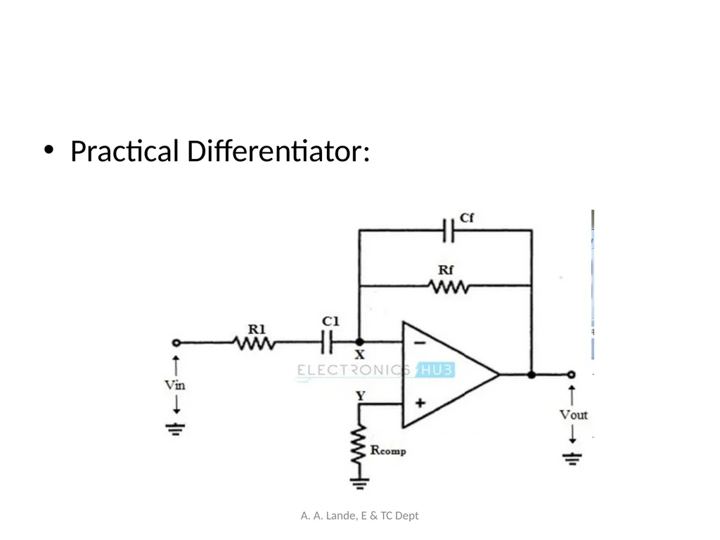
Practical Differentiator: A. A. Lande, E & TC Dept<br>
52
Applications of differentiator:
In the P-I-D controller.
As a high pass filter
In the wave shaping circuits to generate narrow pulses corresponding to any sharp change in the input signal. A. A. Lande, E & TC Dept<br>
In the P-I-D controller.
As a high pass filter
In the wave shaping circuits to generate narrow pulses corresponding to any sharp change in the input signal. A. A. Lande, E & TC Dept<br>
53
Instrumentation Amplifier In many industrial and consumer applications the measurement and control of quantities such as temperature, pressure, humidity etc. is required.
A transducer is used to convert these quantities into a proportional electrical signal first.
Output of the transducer is then applied to an amplifier called “instrumentation amplifier.”
This amplifier amplifies the low level output signal of the transducer to such a level that it can drive the indicator or display. A. A. Lande, E & TC Dept<br>
A transducer is used to convert these quantities into a proportional electrical signal first.
Output of the transducer is then applied to an amplifier called “instrumentation amplifier.”
This amplifier amplifies the low level output signal of the transducer to such a level that it can drive the indicator or display. A. A. Lande, E & TC Dept<br>
54
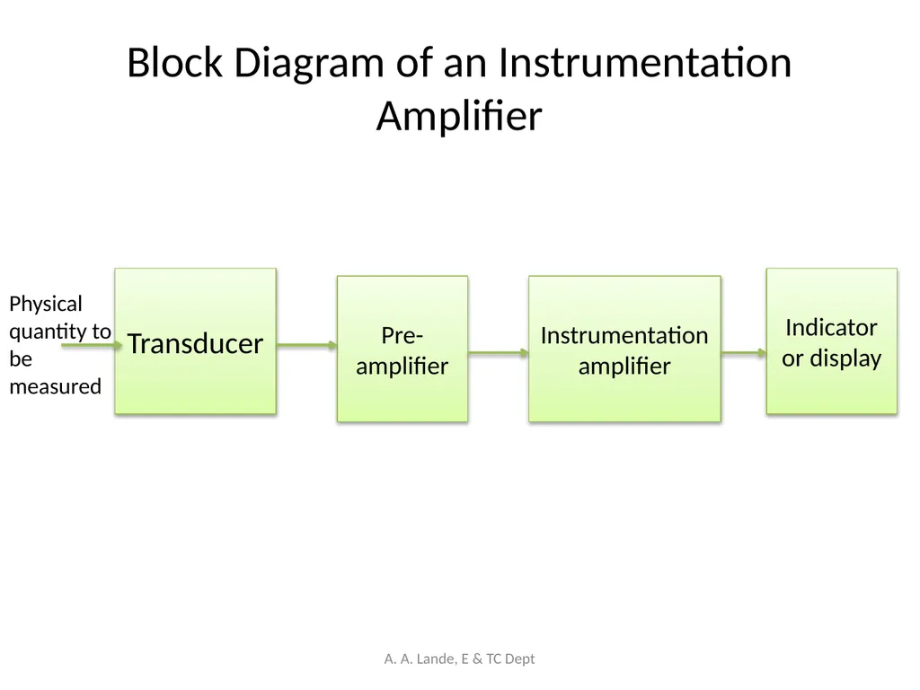
Block Diagram of an Instrumentation Amplifier Transducer Pre-amplifier Instrumentation amplifier Indicator or display Physical quantity to be measured A. A. Lande, E & TC Dept<br>
55
fig. shows the block diagram of instrumentation amplifier.
The transducer is generally connected in a bridge circuit. Its output is amplified using a low noise pre-amplifier and through shielded cables it is applied to an instrumentation amplifier.
Output of the instrumentation amplifier is the amplified version of its input. A. A. Lande, E & TC Dept<br>
The transducer is generally connected in a bridge circuit. Its output is amplified using a low noise pre-amplifier and through shielded cables it is applied to an instrumentation amplifier.
Output of the instrumentation amplifier is the amplified version of its input. A. A. Lande, E & TC Dept<br>
56
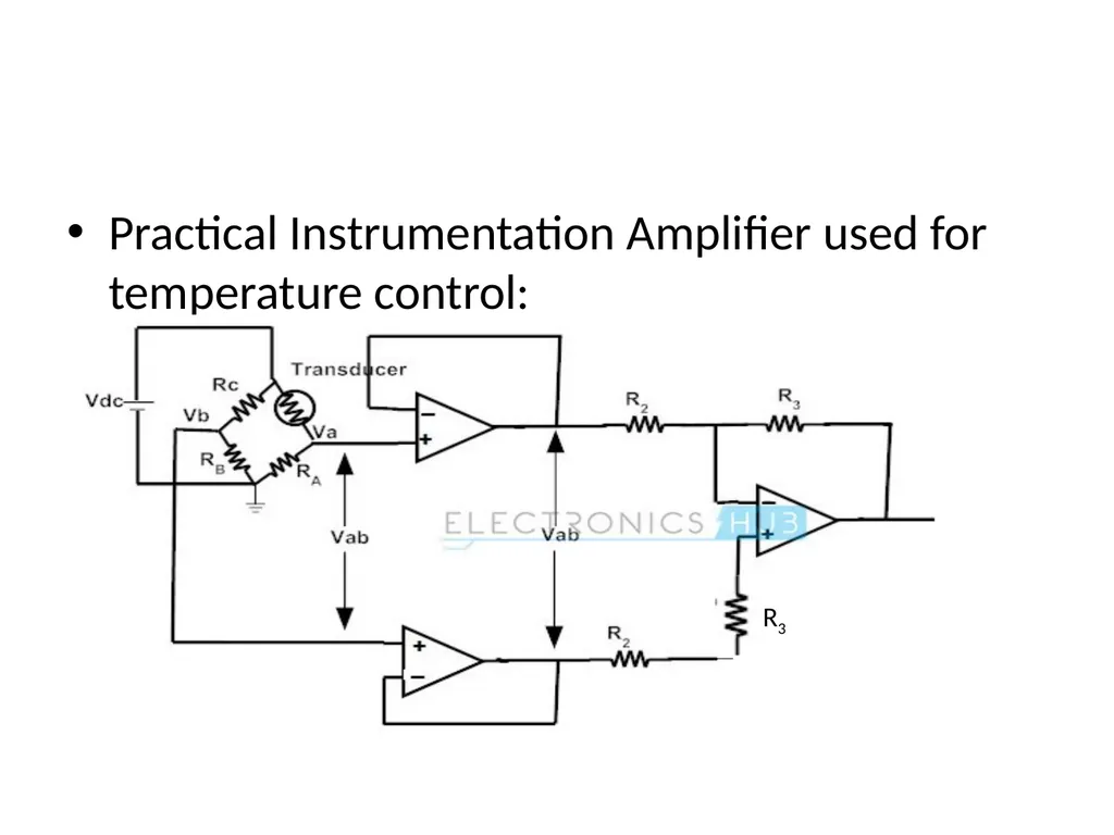
Practical Instrumentation Amplifier used for temperature control: R3 A. A. Lande, E & TC Dept<br>
57
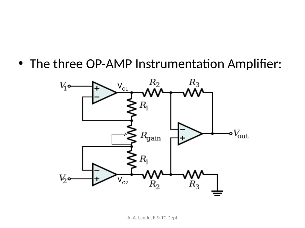
The three OP-AMP Instrumentation Amplifier: VO1 VO2 A. A. Lande, E & TC Dept<br>
58
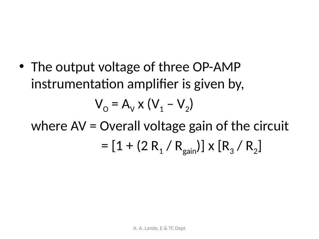
The output voltage of three OP-AMP instrumentation amplifier is given by,
VO = AV x (V1 – V2)
where AV = Overall voltage gain of the circuit
= [1 + (2 R1 / Rgain)] x [R3 / R2] A. A. Lande, E & TC Dept<br>
VO = AV x (V1 – V2)
where AV = Overall voltage gain of the circuit
= [1 + (2 R1 / Rgain)] x [R3 / R2] A. A. Lande, E & TC Dept<br>
59
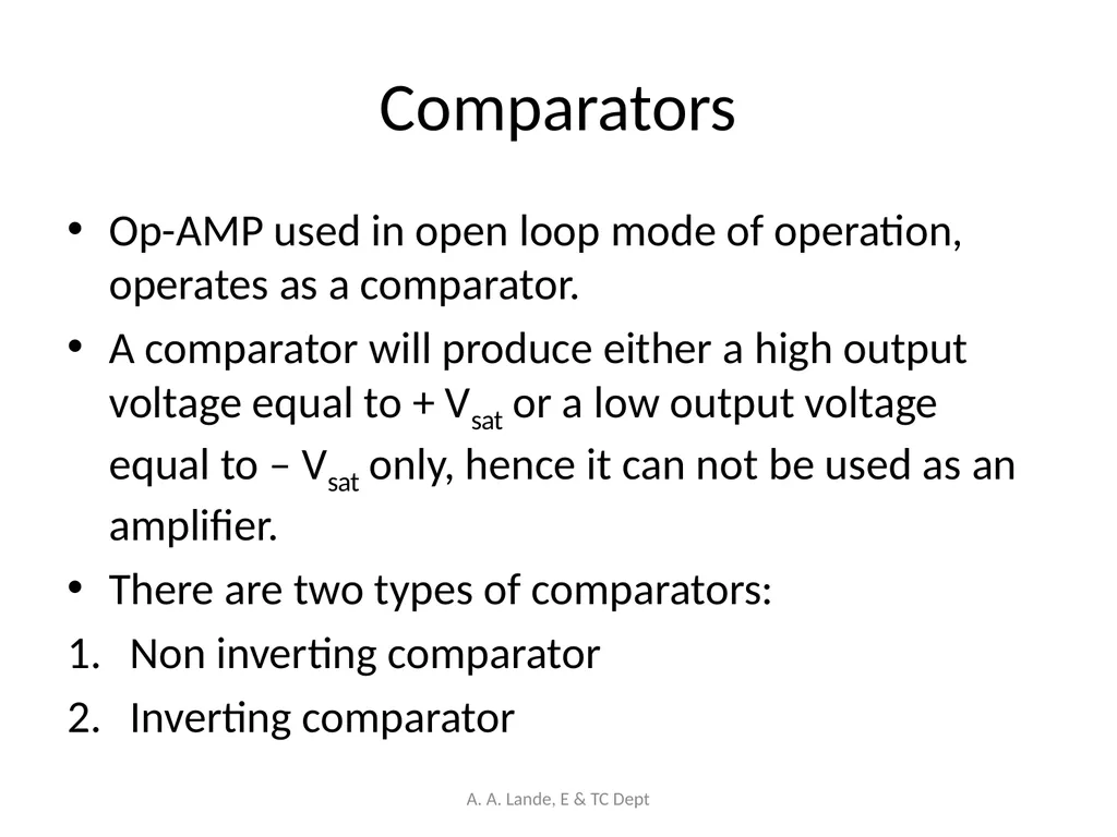
Comparators Op-AMP used in open loop mode of operation, operates as a comparator.
A comparator will produce either a high output voltage equal to + Vsat or a low output voltage equal to – Vsat only, hence it can not be used as an amplifier.
There are two types of comparators:
Non inverting comparator
Inverting comparator A. A. Lande, E & TC Dept<br>
A comparator will produce either a high output voltage equal to + Vsat or a low output voltage equal to – Vsat only, hence it can not be used as an amplifier.
There are two types of comparators:
Non inverting comparator
Inverting comparator A. A. Lande, E & TC Dept<br>
60
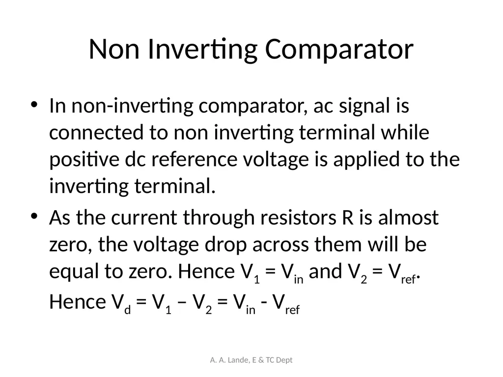
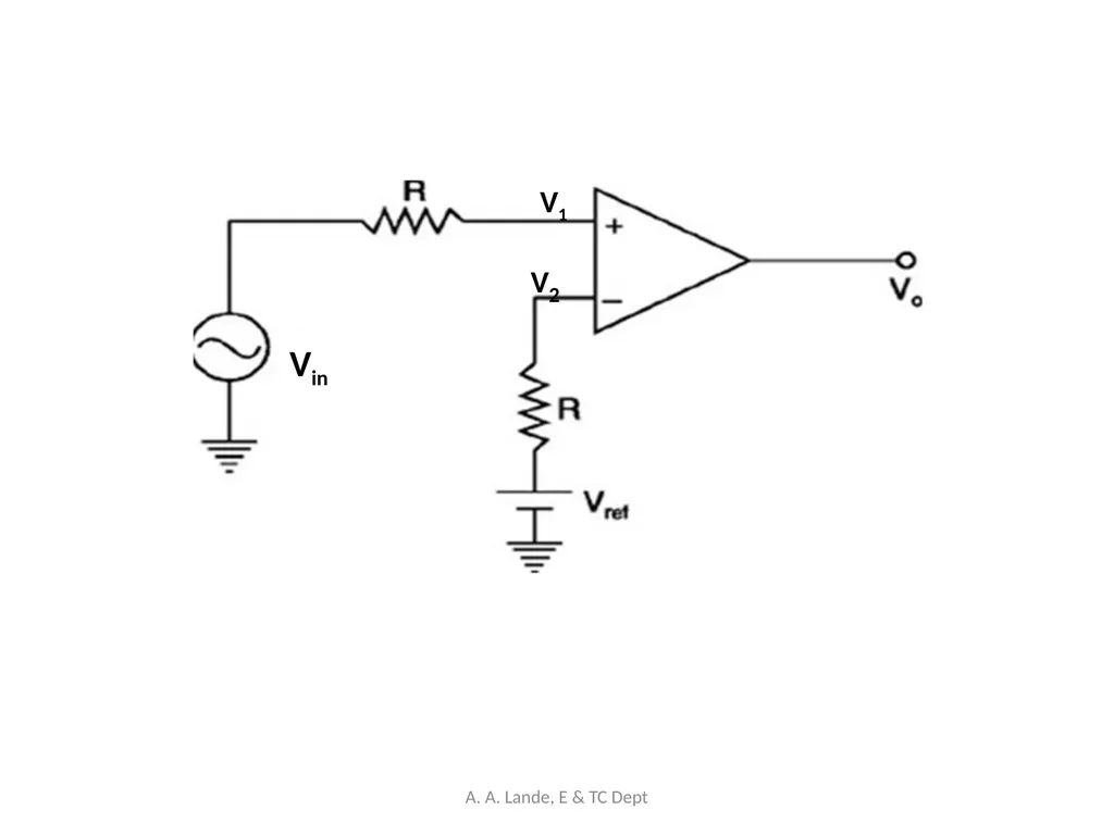
Non Inverting Comparator In non-inverting comparator, ac signal is connected to non inverting terminal while positive dc reference voltage is applied to the inverting terminal.
As the current through resistors R is almost zero, the voltage drop across them will be equal to zero. Hence V1 = Vin and V2 = Vref. Hence Vd = V1 – V2 = Vin - Vref A. A. Lande, E & TC Dept<br>
As the current through resistors R is almost zero, the voltage drop across them will be equal to zero. Hence V1 = Vin and V2 = Vref. Hence Vd = V1 – V2 = Vin - Vref A. A. Lande, E & TC Dept<br>
61
Vin V1 V2 A. A. Lande, E & TC Dept<br>
62
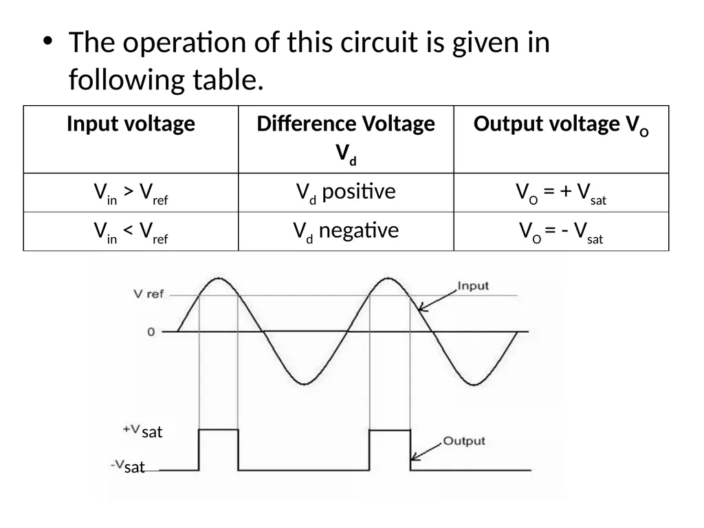
The operation of this circuit is given in following table. sat sat A. A. Lande, E & TC Dept<br>
63
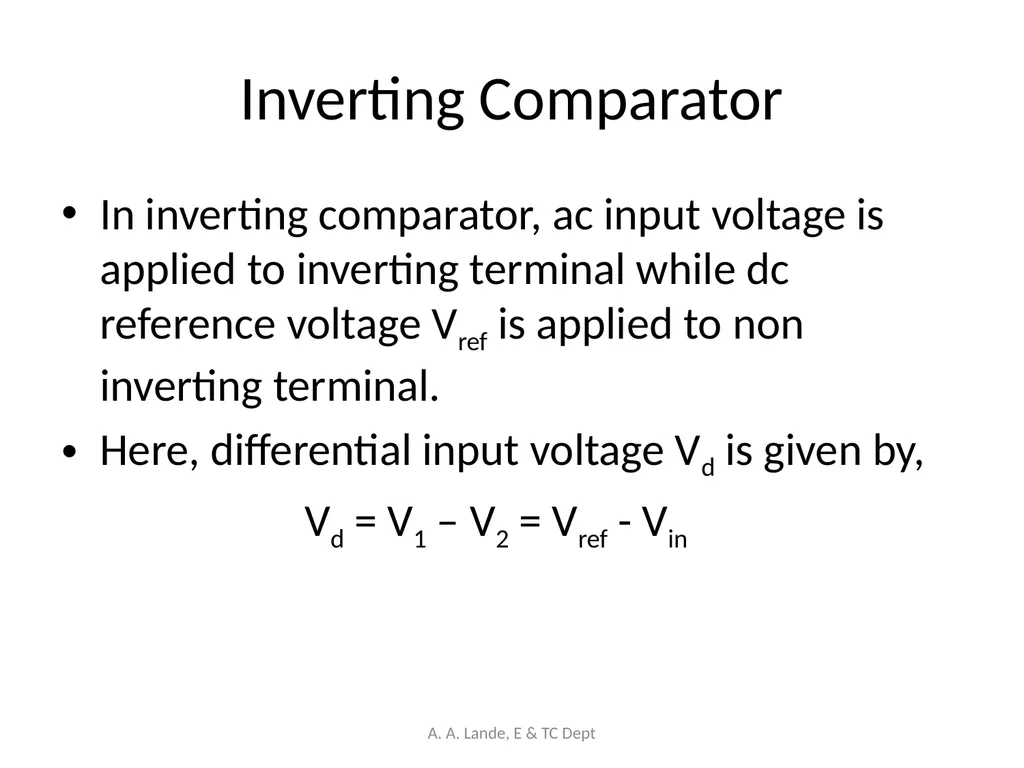
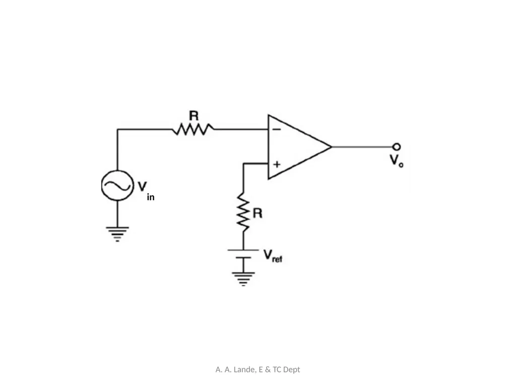
Inverting Comparator In inverting comparator, ac input voltage is applied to inverting terminal while dc reference voltage Vref is applied to non inverting terminal.
Here, differential input voltage Vd is given by,
Vd = V1 – V2 = Vref - Vin A. A. Lande, E & TC Dept<br>
Here, differential input voltage Vd is given by,
Vd = V1 – V2 = Vref - Vin A. A. Lande, E & TC Dept<br>
64
in A. A. Lande, E & TC Dept<br>
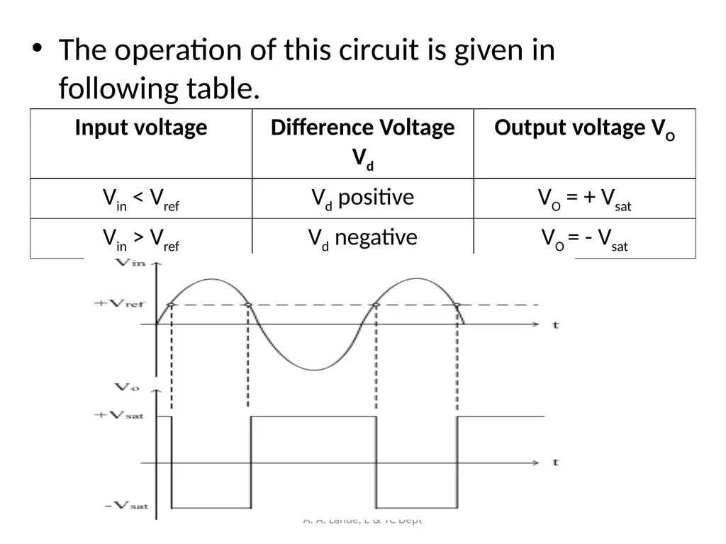
65
The operation of this circuit is given in following table. A. A. Lande, E & TC Dept<br>
66
TIMERS A. A. Lande, E & TC Dept<br>
67
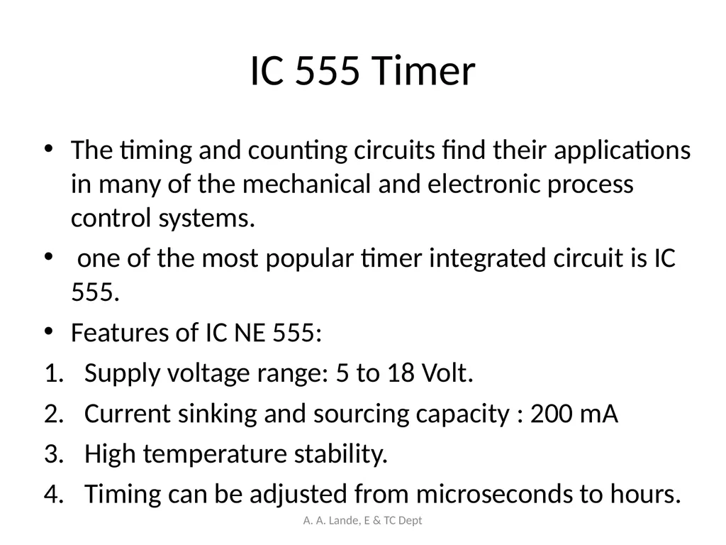
IC 555 Timer The timing and counting circuits find their applications in many of the mechanical and electronic process control systems.
one of the most popular timer integrated circuit is IC 555.
Features of IC NE 555:
Supply voltage range: 5 to 18 Volt.
Current sinking and sourcing capacity : 200 mA
High temperature stability.
Timing can be adjusted from microseconds to hours. A. A. Lande, E & TC Dept<br>
one of the most popular timer integrated circuit is IC 555.
Features of IC NE 555:
Supply voltage range: 5 to 18 Volt.
Current sinking and sourcing capacity : 200 mA
High temperature stability.
Timing can be adjusted from microseconds to hours. A. A. Lande, E & TC Dept<br>
68
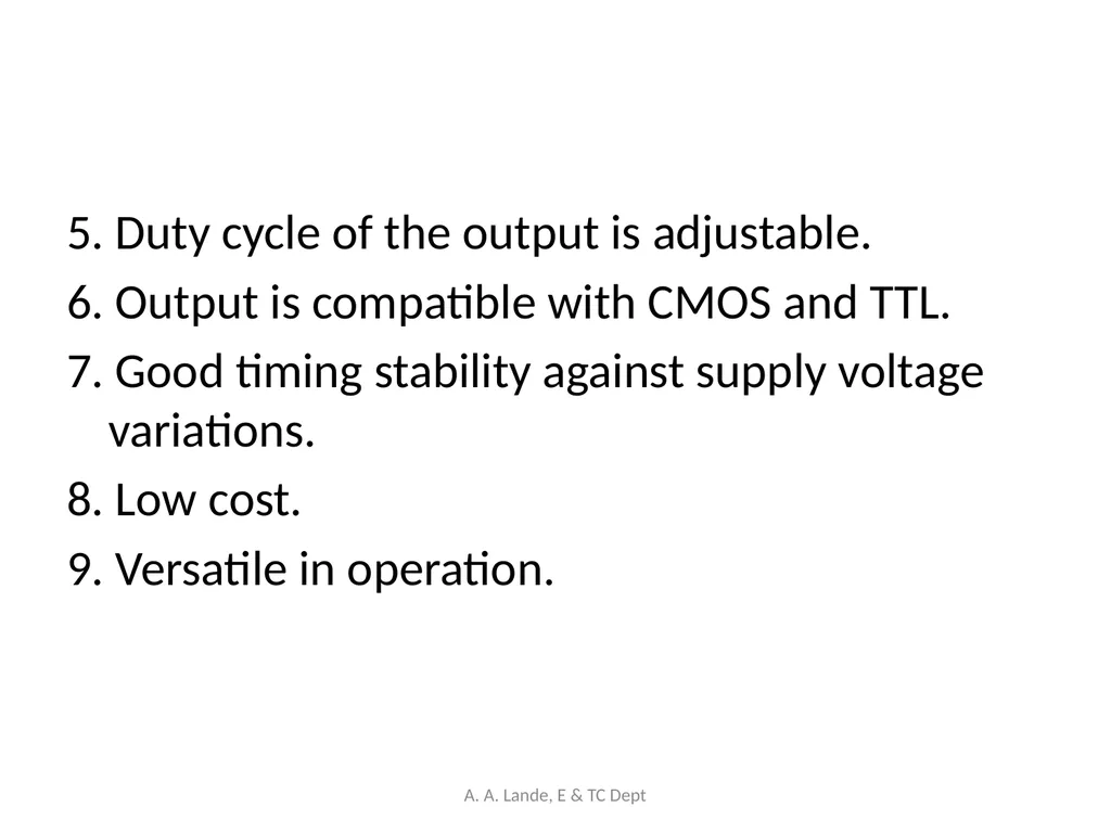
5. Duty cycle of the output is adjustable.
6. Output is compatible with CMOS and TTL.
7. Good timing stability against supply voltage variations.
8. Low cost.
9. Versatile in operation. A. A. Lande, E & TC Dept<br>
6. Output is compatible with CMOS and TTL.
7. Good timing stability against supply voltage variations.
8. Low cost.
9. Versatile in operation. A. A. Lande, E & TC Dept<br>
69
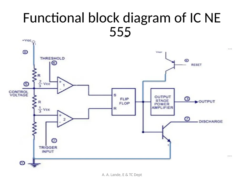
Functional block diagram of IC NE 555 A. A. Lande, E & TC Dept<br>
70
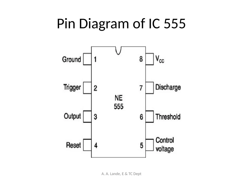
Pin Diagram of IC 555 A. A. Lande, E & TC Dept<br>
71
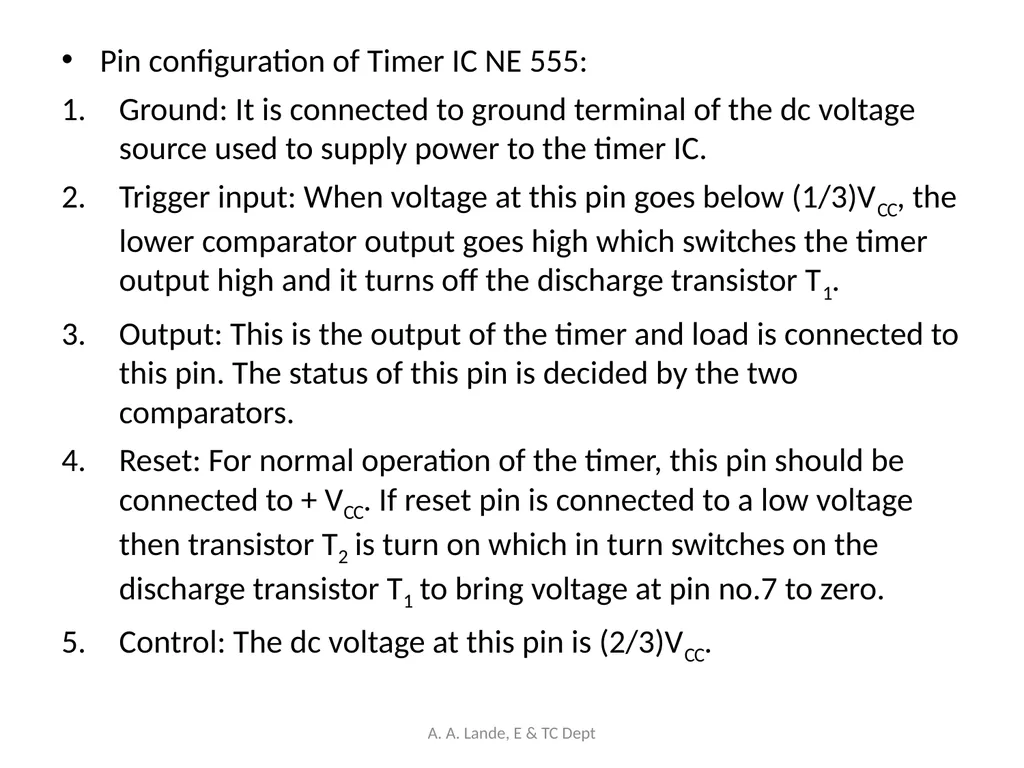
Pin configuration of Timer IC NE 555:
Ground: It is connected to ground terminal of the dc voltage source used to supply power to the timer IC.
Trigger input: When voltage at this pin goes below (1/3)VCC, the lower comparator output goes high which switches the timer output high and it turns off the discharge transistor T1.
Output: This is the output of the timer and load is connected to this pin. The status of this pin is decided by the two comparators.
Reset: For normal operation of the timer, this pin should be connected to + VCC. If reset pin is connected to a low voltage then transistor T2 is turn on which in turn switches on the discharge transistor T1 to bring voltage at pin no.7 to zero.
Control: The dc voltage at this pin is (2/3)VCC. A. A. Lande, E & TC Dept<br>
Ground: It is connected to ground terminal of the dc voltage source used to supply power to the timer IC.
Trigger input: When voltage at this pin goes below (1/3)VCC, the lower comparator output goes high which switches the timer output high and it turns off the discharge transistor T1.
Output: This is the output of the timer and load is connected to this pin. The status of this pin is decided by the two comparators.
Reset: For normal operation of the timer, this pin should be connected to + VCC. If reset pin is connected to a low voltage then transistor T2 is turn on which in turn switches on the discharge transistor T1 to bring voltage at pin no.7 to zero.
Control: The dc voltage at this pin is (2/3)VCC. A. A. Lande, E & TC Dept<br>
72
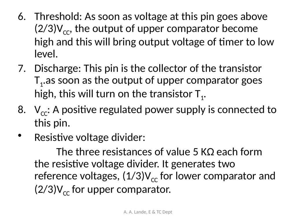
Threshold: As soon as voltage at this pin goes above (2/3)VCC, the output of upper comparator become high and this will bring output voltage of timer to low level.
Discharge: This pin is the collector of the transistor T1.as soon as the output of upper comparator goes high, this will turn on the transistor T1.
VCC: A positive regulated power supply is connected to this pin.
Resistive voltage divider:
The three resistances of value 5 KΩ each form the resistive voltage divider. It generates two reference voltages, (1/3)VCC for lower comparator and (2/3)VCC for upper comparator. A. A. Lande, E & TC Dept<br>
Discharge: This pin is the collector of the transistor T1.as soon as the output of upper comparator goes high, this will turn on the transistor T1.
VCC: A positive regulated power supply is connected to this pin.
Resistive voltage divider:
The three resistances of value 5 KΩ each form the resistive voltage divider. It generates two reference voltages, (1/3)VCC for lower comparator and (2/3)VCC for upper comparator. A. A. Lande, E & TC Dept<br>
73
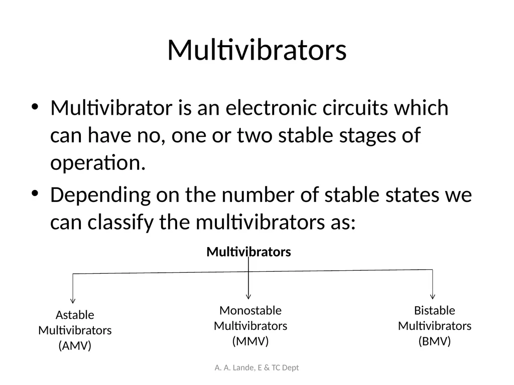
Multivibrators Multivibrator is an electronic circuits which can have no, one or two stable stages of operation.
Depending on the number of stable states we can classify the multivibrators as: Multivibrators Astable Multivibrators (AMV) Monostable Multivibrators (MMV) Bistable Multivibrators (BMV) A. A. Lande, E & TC Dept<br>
Depending on the number of stable states we can classify the multivibrators as: Multivibrators Astable Multivibrators (AMV) Monostable Multivibrators (MMV) Bistable Multivibrators (BMV) A. A. Lande, E & TC Dept<br>
74
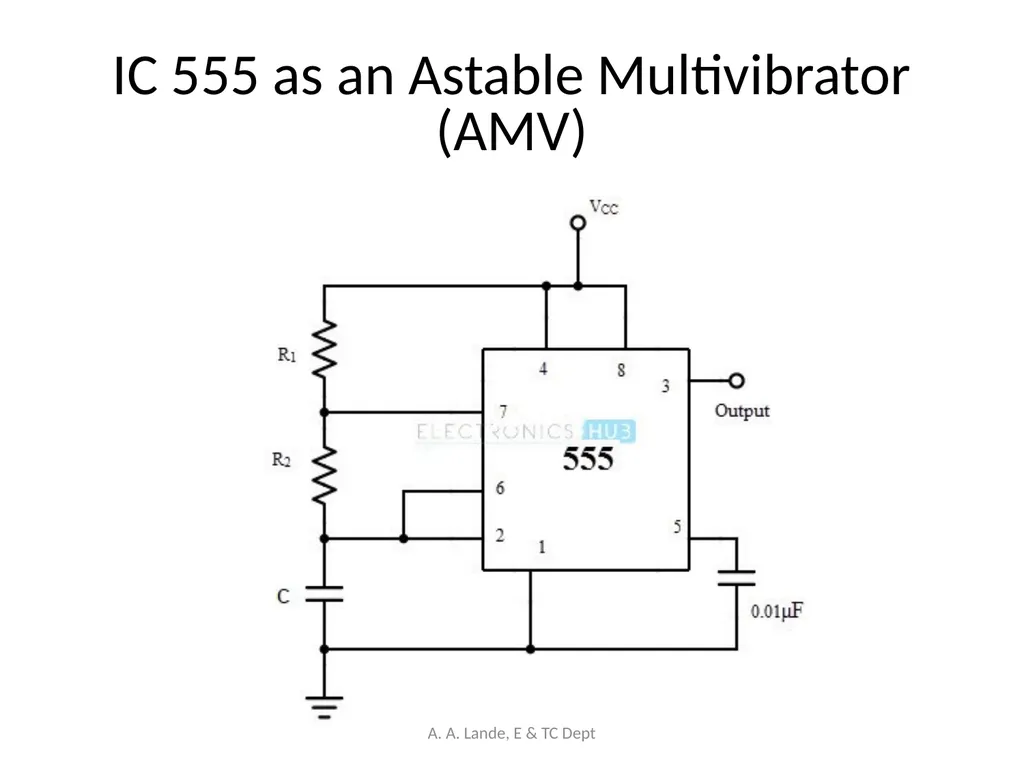
IC 555 as an Astable Multivibrator (AMV) A. A. Lande, E & TC Dept<br>
75
A. A. Lande, E & TC Dept<br>
76
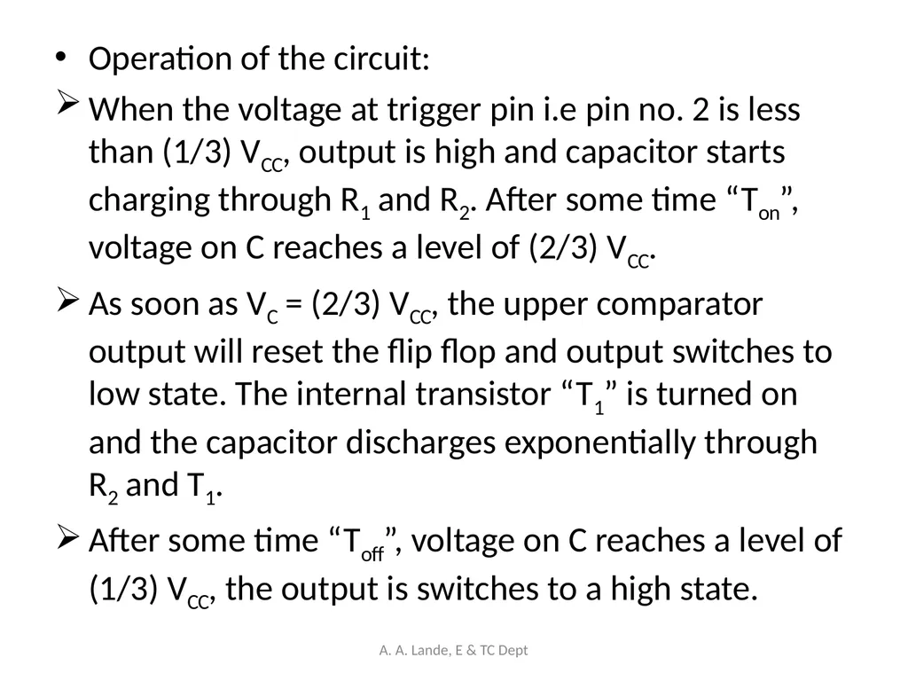
Operation of the circuit:
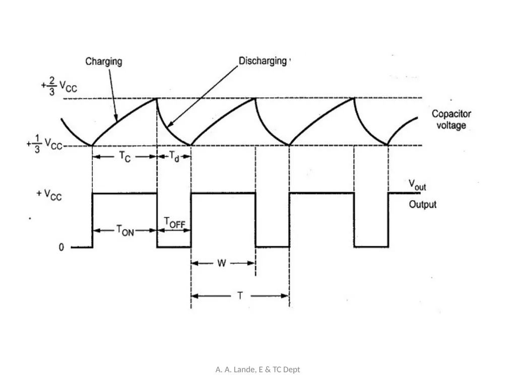
When the voltage at trigger pin i.e pin no. 2 is less than (1/3) VCC, output is high and capacitor starts charging through R1 and R2. After some time “Ton”, voltage on C reaches a level of (2/3) VCC.
As soon as VC = (2/3) VCC, the upper comparator output will reset the flip flop and output switches to low state. The internal transistor “T1” is turned on and the capacitor discharges exponentially through R2 and T1.
After some time “Toff”, voltage on C reaches a level of (1/3) VCC, the output is switches to a high state. A. A. Lande, E & TC Dept<br>
When the voltage at trigger pin i.e pin no. 2 is less than (1/3) VCC, output is high and capacitor starts charging through R1 and R2. After some time “Ton”, voltage on C reaches a level of (2/3) VCC.
As soon as VC = (2/3) VCC, the upper comparator output will reset the flip flop and output switches to low state. The internal transistor “T1” is turned on and the capacitor discharges exponentially through R2 and T1.
After some time “Toff”, voltage on C reaches a level of (1/3) VCC, the output is switches to a high state. A. A. Lande, E & TC Dept<br>
77
Applications of astable multivibrator:
Square wave oscillator
Ramp generator
Voltage controlled oscillator
In the flasher circuit A. A. Lande, E & TC Dept<br>
Square wave oscillator
Ramp generator
Voltage controlled oscillator
In the flasher circuit A. A. Lande, E & TC Dept<br>
78
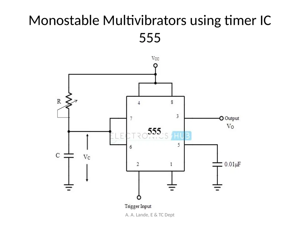
Monostable Multivibrators using timer IC 555 A. A. Lande, E & TC Dept<br>
79
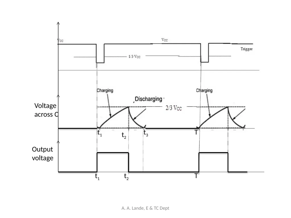
Voltage across C Output voltage t1 t2 t3 t1 t2 T T A. A. Lande, E & TC Dept<br>
80
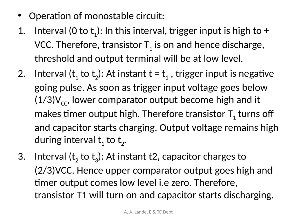
Operation of monostable circuit:
Interval (0 to t1): In this interval, trigger input is high to + VCC. Therefore, transistor T1 is on and hence discharge, threshold and output terminal will be at low level.
Interval (t1 to t2): At instant t = t1 , trigger input is negative going pulse. As soon as trigger input voltage goes below (1/3)VCC, lower comparator output become high and it makes timer output high. Therefore transistor T1 turns off and capacitor starts charging. Output voltage remains high during interval t1 to t2.
Interval (t2 to t3): At instant t2, capacitor charges to (2/3)VCC. Hence upper comparator output goes high and timer output comes low level i.e zero. Therefore, transistor T1 will turn on and capacitor starts discharging. A. A. Lande, E & TC Dept<br>
Interval (0 to t1): In this interval, trigger input is high to + VCC. Therefore, transistor T1 is on and hence discharge, threshold and output terminal will be at low level.
Interval (t1 to t2): At instant t = t1 , trigger input is negative going pulse. As soon as trigger input voltage goes below (1/3)VCC, lower comparator output become high and it makes timer output high. Therefore transistor T1 turns off and capacitor starts charging. Output voltage remains high during interval t1 to t2.
Interval (t2 to t3): At instant t2, capacitor charges to (2/3)VCC. Hence upper comparator output goes high and timer output comes low level i.e zero. Therefore, transistor T1 will turn on and capacitor starts discharging. A. A. Lande, E & TC Dept<br>
81
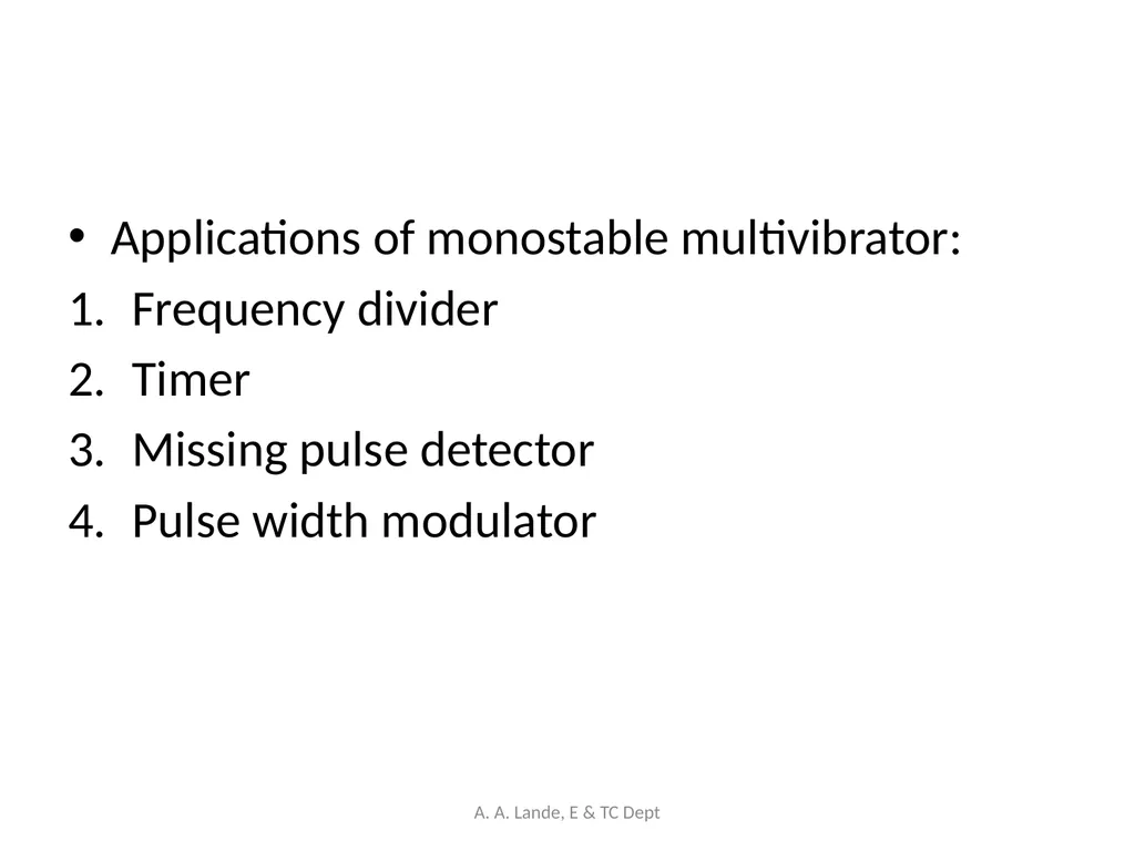
Applications of monostable multivibrator:
Frequency divider
Timer
Missing pulse detector
Pulse width modulator A. A. Lande, E & TC Dept<br>
Frequency divider
Timer
Missing pulse detector
Pulse width modulator A. A. Lande, E & TC Dept<br>
82
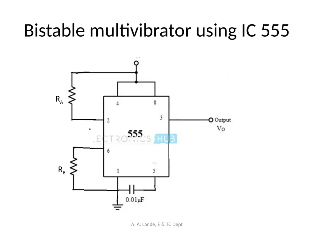
Bistable multivibrator using IC 555 RA RB A. A. Lande, E & TC Dept<br>
83
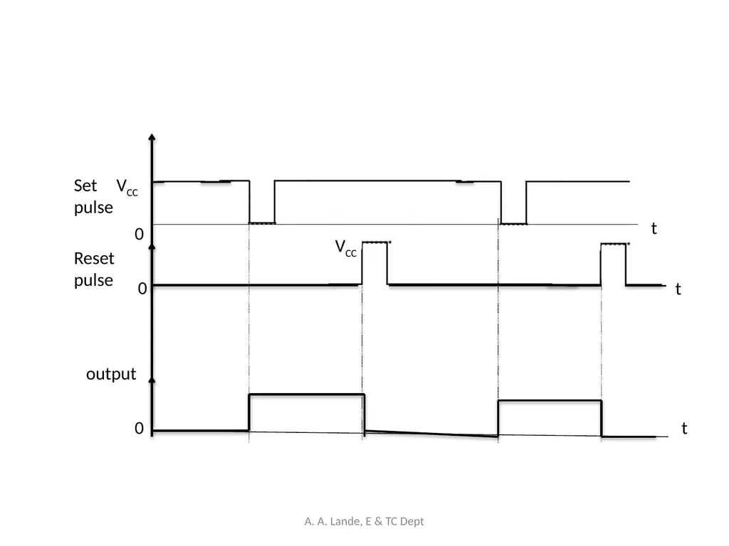
0 0 0 VCC VCC Set pulse Reset pulse output t t t A. A. Lande, E & TC Dept<br>
84
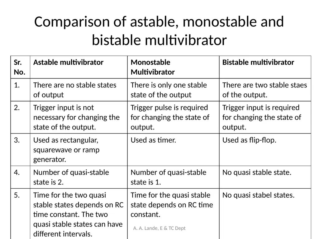
Comparison of astable, monostable and bistable multivibrator A. A. Lande, E & TC Dept<br>
85
Applications of IC 555 As adomestic timer.
As a sequential timer in industrial application.
Ramp generator.
Square wave / recangular wave generator.
Missing pulse detector.
Schmitt trigger.
FSK generator. A. A. Lande, E & TC Dept<br>
As a sequential timer in industrial application.
Ramp generator.
Square wave / recangular wave generator.
Missing pulse detector.
Schmitt trigger.
FSK generator. A. A. Lande, E & TC Dept<br>
86
OSCILLATORS A. A. Lande, E & TC Dept<br>
87
Introduction Feedback is defined as the process in which a part of output signal is returned back to the input.
Types of feedback:
Positive feedback 2. Negative feedback
If the original input signal and feedback signal are in phase, the feedback is called as “positive feedback”.
Positive feedback is used in oscillators. A. A. Lande, E & TC Dept<br>
Types of feedback:
Positive feedback 2. Negative feedback
If the original input signal and feedback signal are in phase, the feedback is called as “positive feedback”.
Positive feedback is used in oscillators. A. A. Lande, E & TC Dept<br>
88
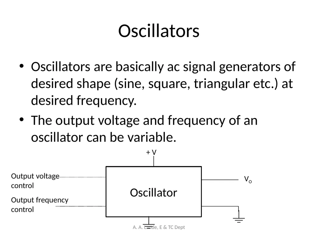
Oscillators Oscillators are basically ac signal generators of desired shape (sine, square, triangular etc.) at desired frequency.
The output voltage and frequency of an oscillator can be variable. Oscillator + V Output voltage control Output frequency control VO A. A. Lande, E & TC Dept<br>
The output voltage and frequency of an oscillator can be variable. Oscillator + V Output voltage control Output frequency control VO A. A. Lande, E & TC Dept<br>
89
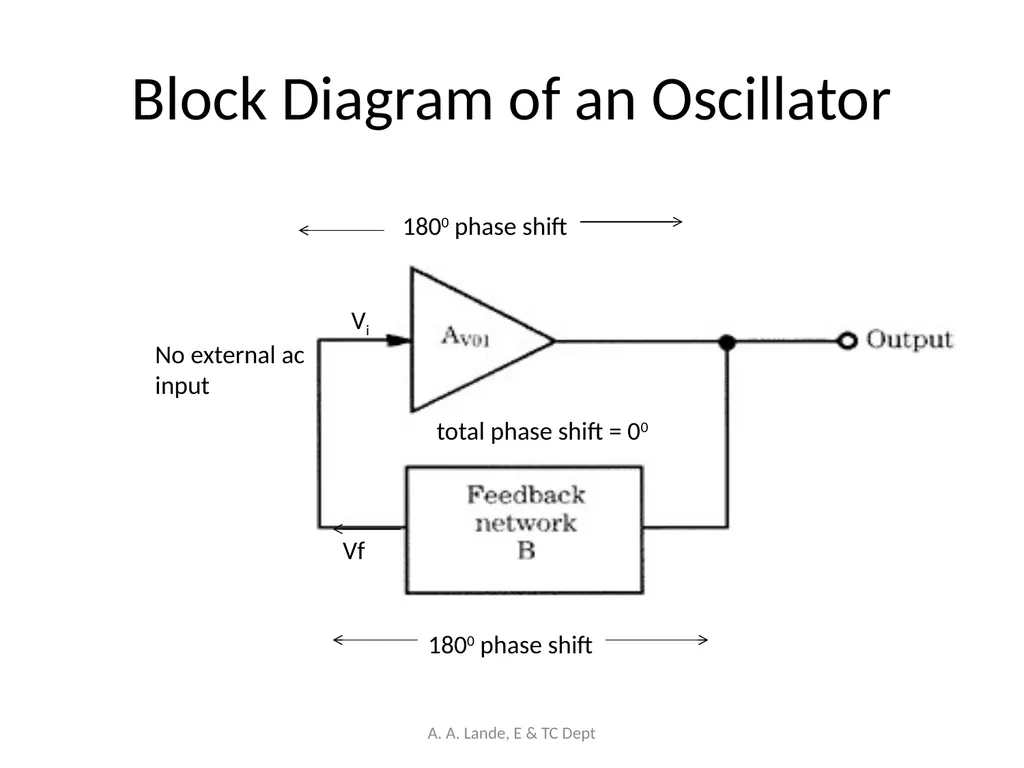
Block Diagram of an Oscillator 1800 phase shift 1800 phase shift total phase shift = 00 Vi Vf No external ac input A. A. Lande, E & TC Dept<br>
90
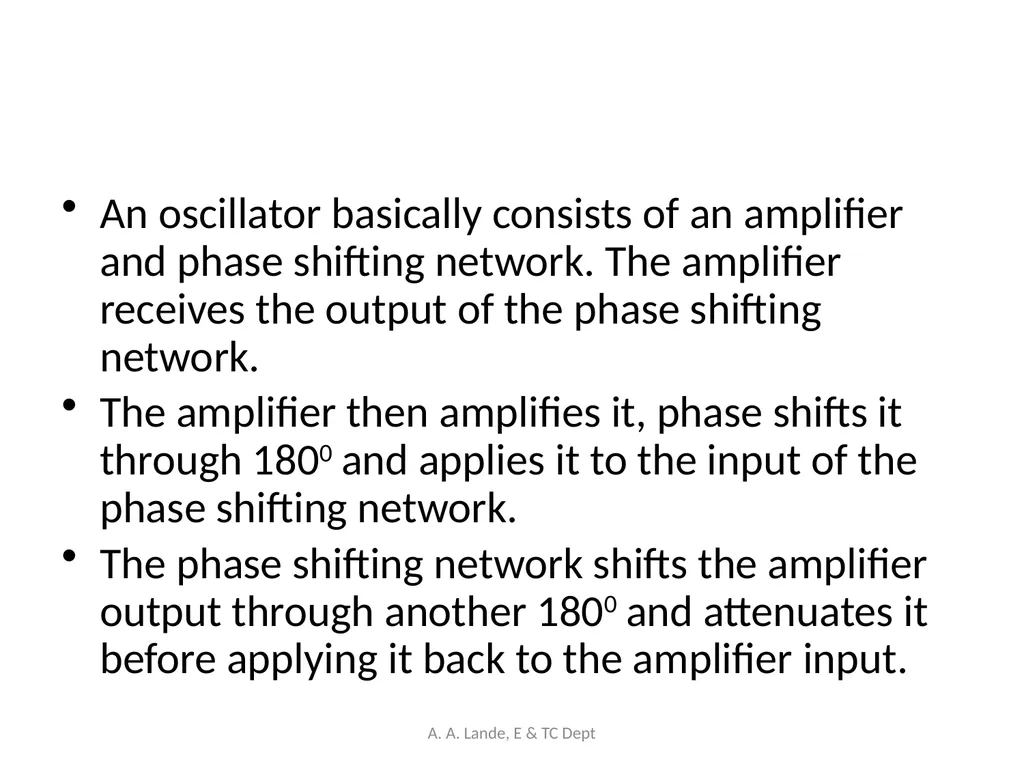
An oscillator basically consists of an amplifier and phase shifting network. The amplifier receives the output of the phase shifting network.
The amplifier then amplifies it, phase shifts it through 1800 and applies it to the input of the phase shifting network.
The phase shifting network shifts the amplifier output through another 1800 and attenuates it before applying it back to the amplifier input. A. A. Lande, E & TC Dept<br>
The amplifier then amplifies it, phase shifts it through 1800 and applies it to the input of the phase shifting network.
The phase shifting network shifts the amplifier output through another 1800 and attenuates it before applying it back to the amplifier input. A. A. Lande, E & TC Dept<br>
91
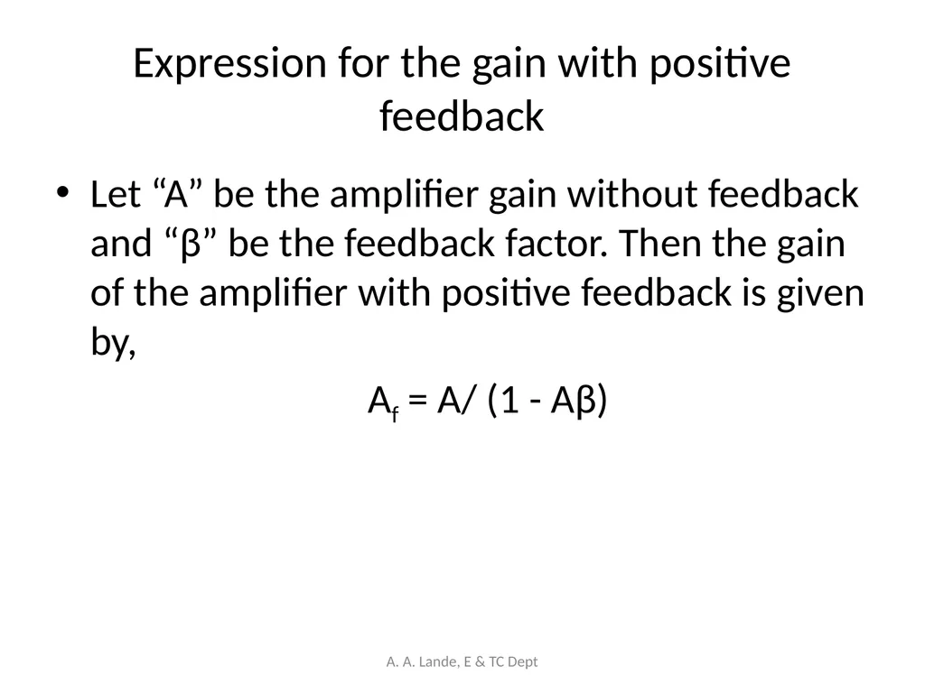
Expression for the gain with positive feedback Let “A” be the amplifier gain without feedback and “β” be the feedback factor. Then the gain of the amplifier with positive feedback is given by,
Af = A/ (1 - Aβ) A. A. Lande, E & TC Dept<br>
Af = A/ (1 - Aβ) A. A. Lande, E & TC Dept<br>
92
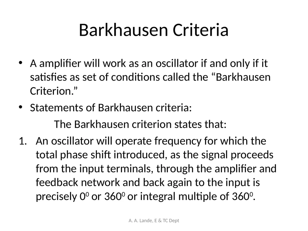
Barkhausen Criteria A amplifier will work as an oscillator if and only if it satisfies as set of conditions called the “Barkhausen Criterion.”
Statements of Barkhausen criteria:
The Barkhausen criterion states that:
An oscillator will operate frequency for which the total phase shift introduced, as the signal proceeds from the input terminals, through the amplifier and feedback network and back again to the input is precisely 00 or 3600 or integral multiple of 3600. A. A. Lande, E & TC Dept<br>
Statements of Barkhausen criteria:
The Barkhausen criterion states that:
An oscillator will operate frequency for which the total phase shift introduced, as the signal proceeds from the input terminals, through the amplifier and feedback network and back again to the input is precisely 00 or 3600 or integral multiple of 3600. A. A. Lande, E & TC Dept<br>
93
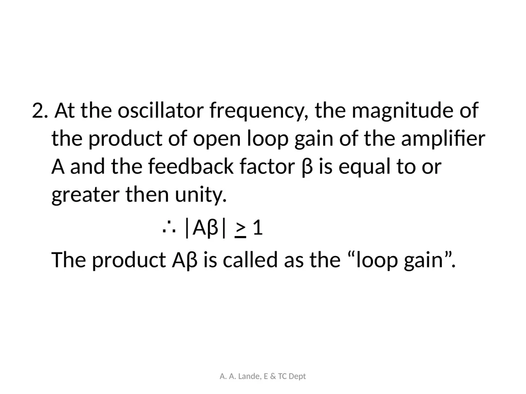
2. At the oscillator frequency, the magnitude of the product of open loop gain of the amplifier A and the feedback factor β is equal to or greater then unity.
∴ |Aβ| > 1
The product Aβ is called as the “loop gain”. A. A. Lande, E & TC Dept<br>
∴ |Aβ| > 1
The product Aβ is called as the “loop gain”. A. A. Lande, E & TC Dept<br>
94
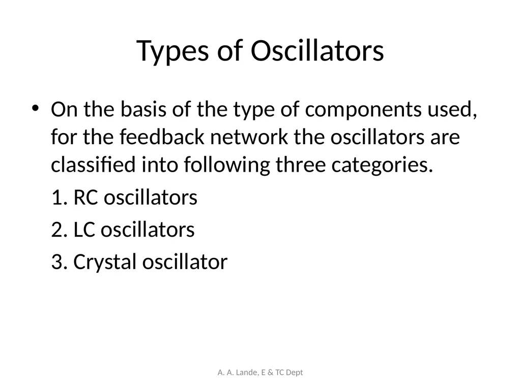
Types of Oscillators On the basis of the type of components used, for the feedback network the oscillators are classified into following three categories.
1. RC oscillators
2. LC oscillators
3. Crystal oscillator A. A. Lande, E & TC Dept<br>
1. RC oscillators
2. LC oscillators
3. Crystal oscillator A. A. Lande, E & TC Dept<br>
95
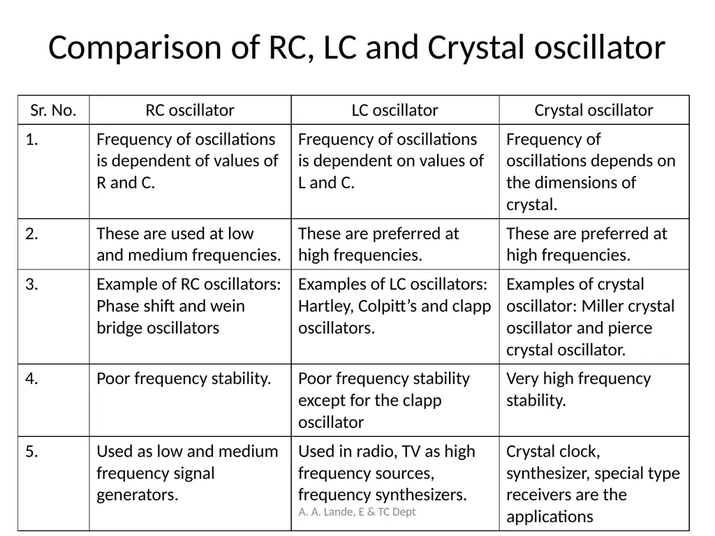
Comparison of RC, LC and Crystal oscillator A. A. Lande, E & TC Dept<br>
96
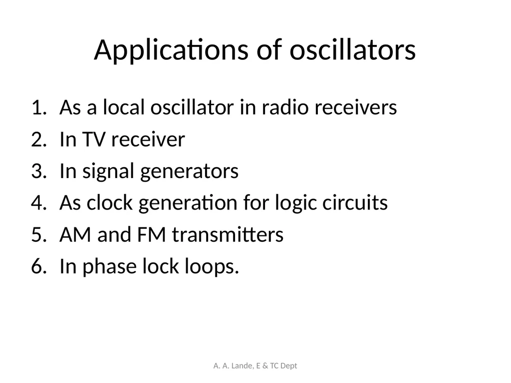
Applications of oscillators As a local oscillator in radio receivers
In TV receiver
In signal generators
As clock generation for logic circuits
AM and FM transmitters
In phase lock loops. A. A. Lande, E & TC Dept<br>
In TV receiver
In signal generators
As clock generation for logic circuits
AM and FM transmitters
In phase lock loops. A. A. Lande, E & TC Dept<br>