
Auger Electron Spectroscopy Overview Also known
Description: Auger Electron Spectroscopy Overview Also known as: AES, Auger, SAM 1 Auger Electron Spectroscopy EKLL EK - EL - EL AES Spectra of Cu Note that Auger peaks are typically superimposed on a large background (see red and magenta spectra).
Related Topics
Download Presentation
"Auger Electron Spectroscopy Overview Also known" is the property of its rightful owner. Permission is granted to download and print the materials on this website for personal, non-commercial use only, and to display it on your personal computer provided you do not modify the materials and that you retain all copyright notices contained in the materials. By downloading content from our website, you accept the terms of this agreement.
Presentation Transcript
slide1. Auger Electron Spectroscopy Overview Also known as: AES, Auger, SAM 1<br>
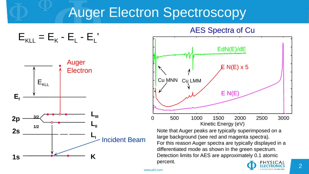
slide2. Auger Electron Spectroscopy EKLL = EK - EL - EL’ AES Spectra of Cu Note that Auger peaks are typically superimposed on a large background (see red and magenta spectra).
For this reason Auger spectra are typically displayed in a differentiated mode as shown in the green spectrum.
Detection limits for AES are approximately 0.1 atomic percent. 2<br>
slide3. Auger Electron and X-ray Emission Incident
Beam Auger Electron X-ray
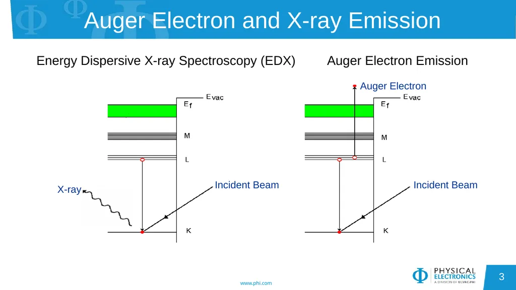
Photon Energy Dispersive X-ray Spectroscopy (EDX) Auger Electron Emission Incident Beam Incident Beam Auger Electron X-ray 3<br>
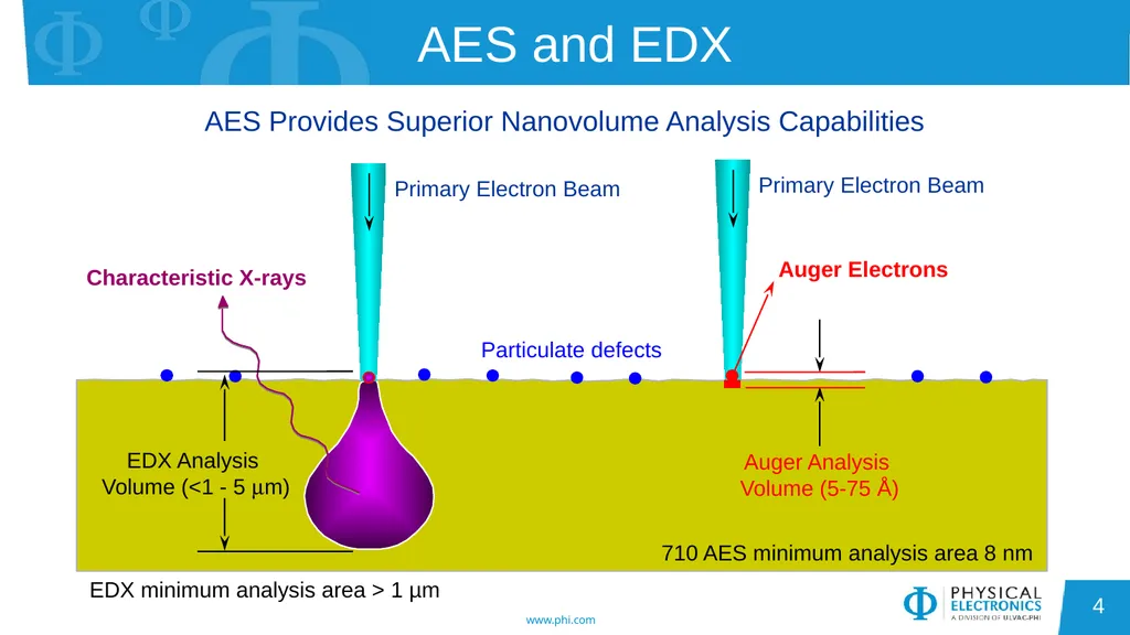
slide4. AES and EDX AES Provides Superior Nanovolume Analysis Capabilities EDX minimum analysis area > 1 µm 710 AES minimum analysis area 8 nm 4<br>
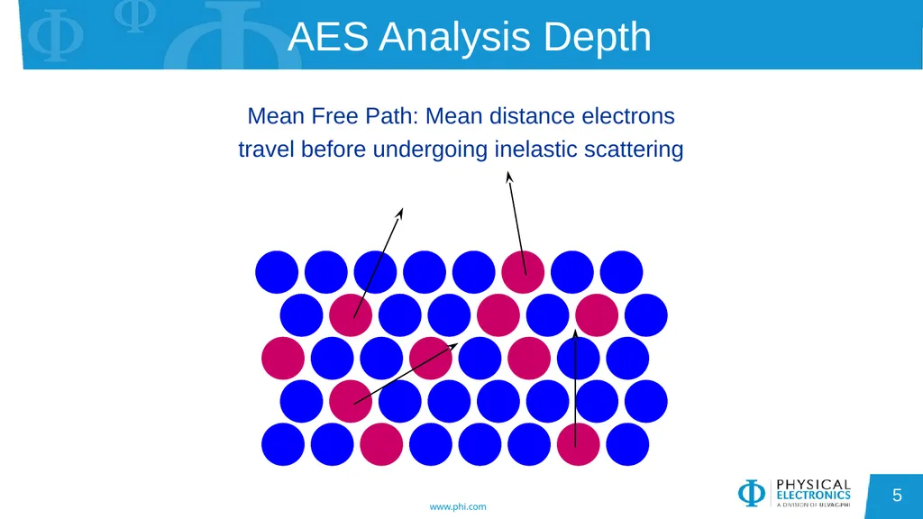
slide5. AES Analysis Depth Mean Free Path: Mean distance electrons travel before undergoing inelastic scattering 5<br>
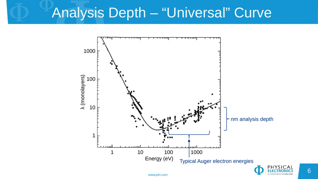
slide6. Analysis Depth – “Universal” Curve 6<br>
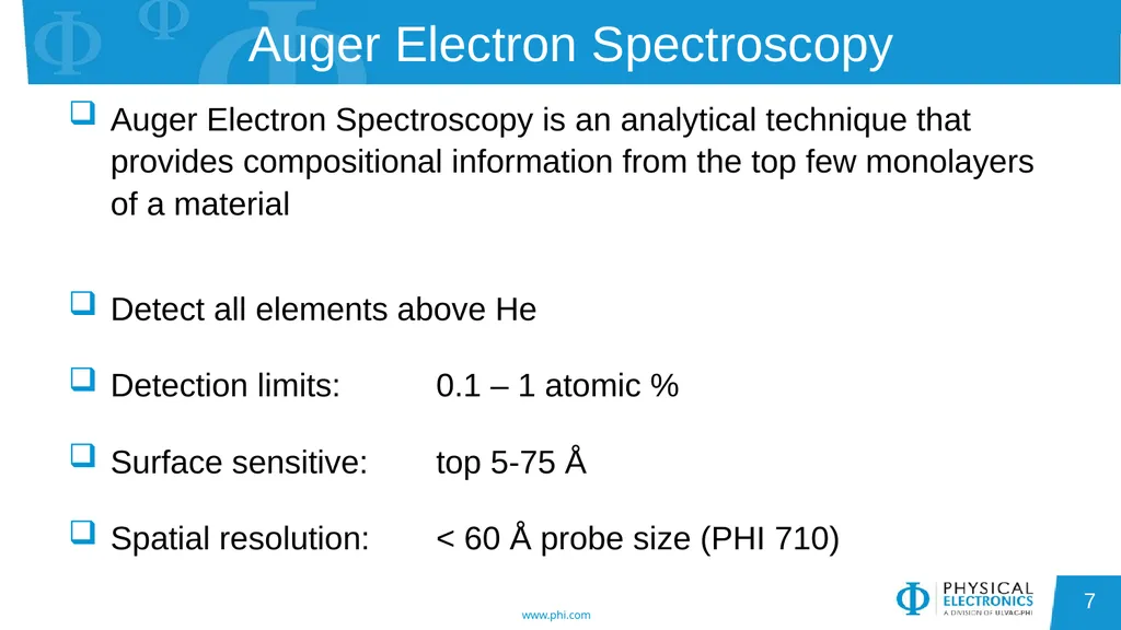
slide7. Auger Electron Spectroscopy Auger Electron Spectroscopy is an analytical technique that provides compositional information from the top few monolayers of a material
Detect all elements above He
Detection limits: 0.1 – 1 atomic %
Surface sensitive: top 5-75 Å
Spatial resolution: < 60 Å probe size (PHI 710) 7<br>
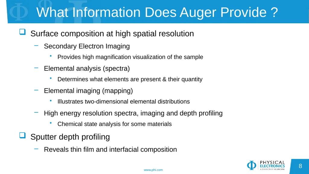
slide8. What Information Does Auger Provide ? Surface composition at high spatial resolution
Secondary Electron Imaging
Provides high magnification visualization of the sample
Elemental analysis (spectra)
Determines what elements are present & their quantity
Elemental imaging (mapping)
Illustrates two-dimensional elemental distributions
High energy resolution spectra, imaging and depth profiling
Chemical state analysis for some materials
Sputter depth profiling
Reveals thin film and interfacial composition 8<br>
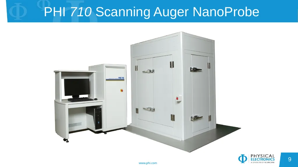
slide9. PHI 710 Scanning Auger NanoProbe 9<br>
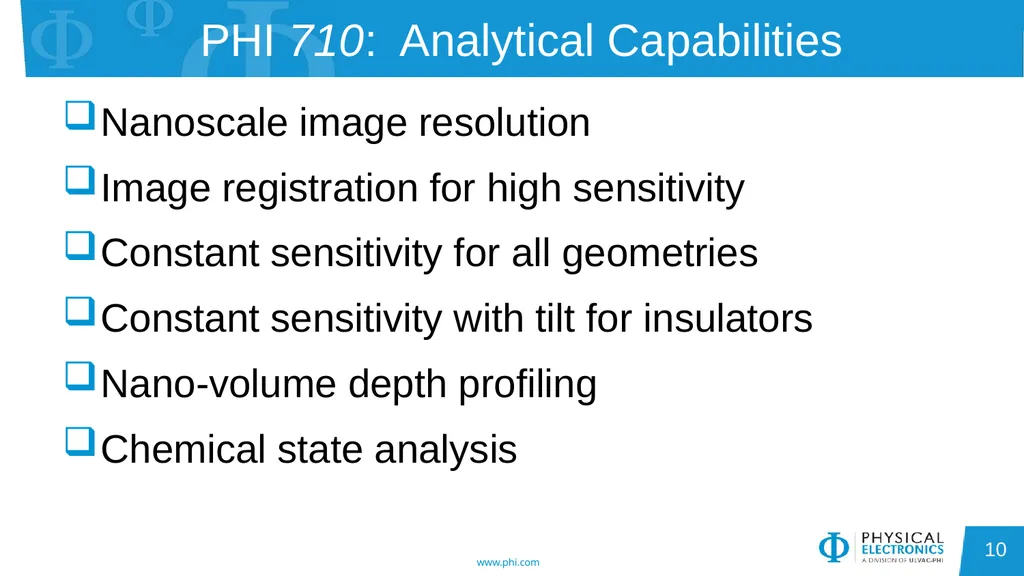
slide10. PHI 710: Analytical Capabilities Nanoscale image resolution
Image registration for high sensitivity
Constant sensitivity for all geometries
Constant sensitivity with tilt for insulators
Nano-volume depth profiling
Chemical state analysis 10<br>
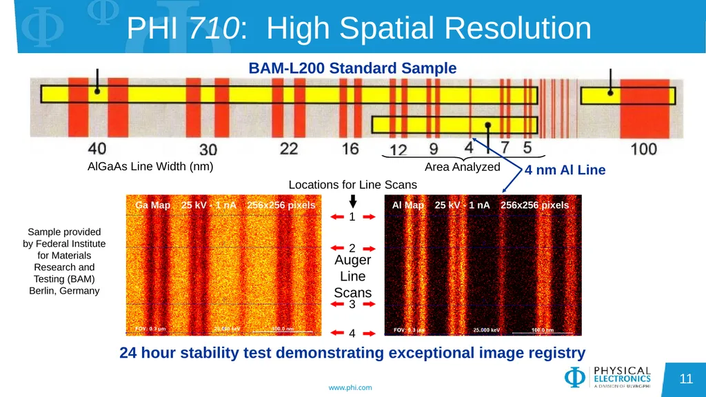
slide11. PHI 710: High Spatial Resolution Locations for Line Scans Area Analyzed 4 nm Al Line AlGaAs Line Width (nm) Auger
Line
Scans Sample provided by Federal Institute for Materials Research and Testing (BAM)
Berlin, Germany 24 hour stability test demonstrating exceptional image registry BAM-L200 Standard Sample Ga Map 25 kV - 1 nA 256x256 pixels Al Map 25 kV - 1 nA 256x256 pixels 11<br>
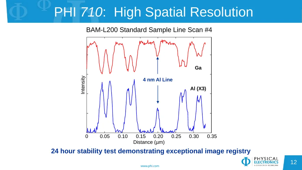
slide12. PHI 710: High Spatial Resolution 4 nm Al Line 0 0.05 0.10 0.15 0.20 0.25 0.30 0.35 Distance (µm) Intensity Ga Al (X3) BAM-L200 Standard Sample Line Scan #4 24 hour stability test demonstrating exceptional image registry 12<br>
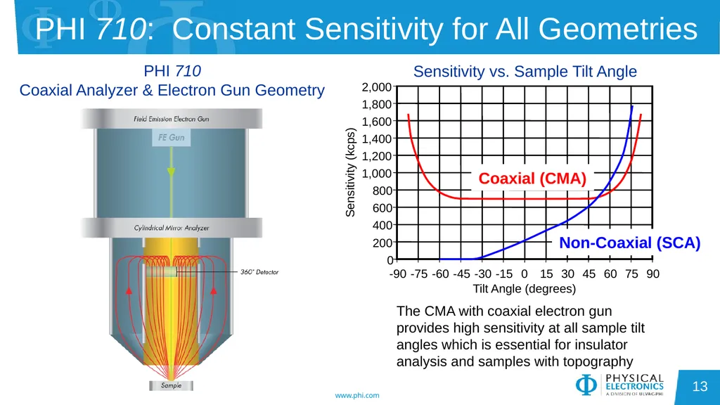
slide13. PHI 710: Constant Sensitivity for All Geometries PHI 710
Coaxial Analyzer & Electron Gun Geometry The CMA with coaxial electron gun provides high sensitivity at all sample tilt angles which is essential for insulator analysis and samples with topography 13<br>
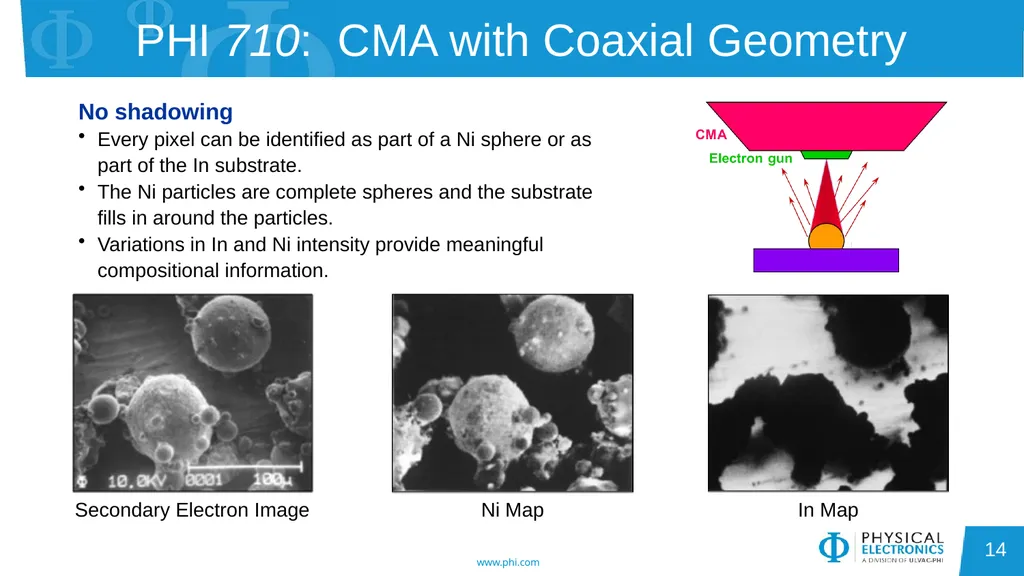
slide14. PHI 710: CMA with Coaxial Geometry Secondary Electron Image Ni Map In Map No shadowing
Every pixel can be identified as part of a Ni sphere or as part of the In substrate.
The Ni particles are complete spheres and the substrate fills in around the particles.
Variations in In and Ni intensity provide meaningful compositional information. 14<br>
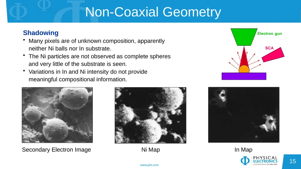
slide15. Non-Coaxial Geometry Secondary Electron Image Ni Map In Map Shadowing
Many pixels are of unknown composition, apparently neither Ni balls nor In substrate.
The Ni particles are not observed as complete spheres and very little of the substrate is seen.
Variations in In and Ni intensity do not provide meaningful compositional information. 15<br>
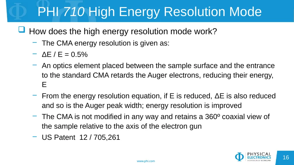
slide16. PHI 710 High Energy Resolution Mode How does the high energy resolution mode work?
The CMA energy resolution is given as:
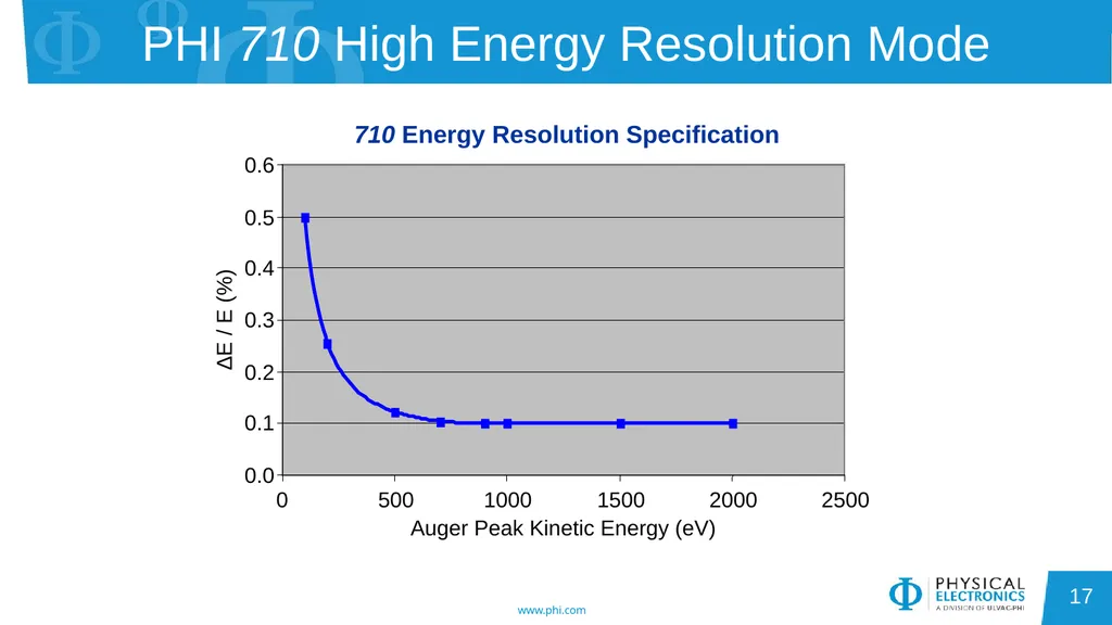
ΔE / E = 0.5%
An optics element placed between the sample surface and the entrance to the standard CMA retards the Auger electrons, reducing their energy, E
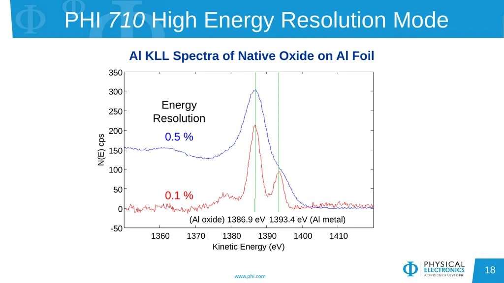
From the energy resolution equation, if E is reduced, ΔE is also reduced and so is the Auger peak width; energy resolution is improved
The CMA is not modified in any way and retains a 360º coaxial view of the sample relative to the axis of the electron gun
US Patent 12 / 705,261 16<br>
slide17. PHI 710 High Energy Resolution Mode 17<br>
slide18. PHI 710 High Energy Resolution Mode 1360 1370 1380 1390 1400 1410 -50 0 50 100 150 200 250 300 350 1393.4 eV (Al metal) (Al oxide) 1386.9 eV Kinetic Energy (eV) N(E) cps Al KLL Spectra of Native Oxide on Al Foil Energy
Resolution 0.5 % 0.1 % 18<br>
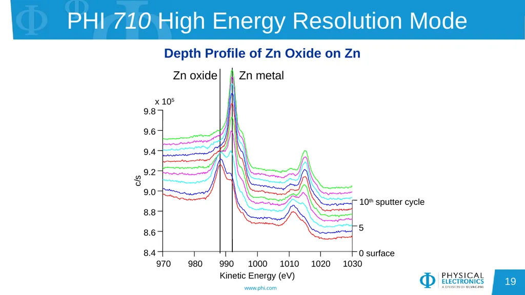
slide19. PHI 710 High Energy Resolution Mode Depth Profile of Zn Oxide on Zn 19<br>
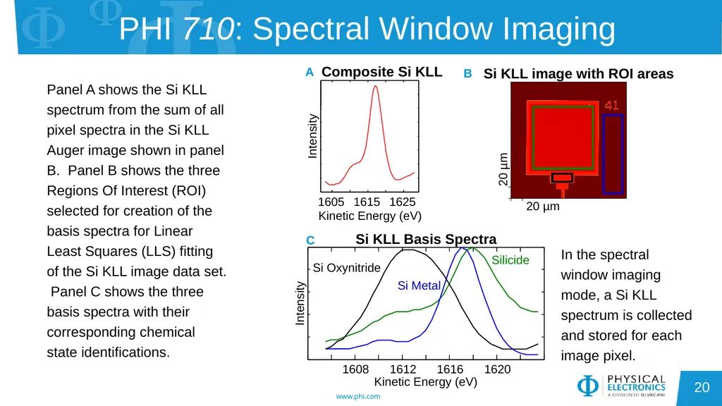
slide20. PHI 710: Spectral Window Imaging B Panel A shows the Si KLL spectrum from the sum of all pixel spectra in the Si KLL Auger image shown in panel B. Panel B shows the three Regions Of Interest (ROI) selected for creation of the basis spectra for Linear Least Squares (LLS) fitting of the Si KLL image data set. Panel C shows the three basis spectra with their corresponding chemical state identifications. In the spectral window imaging mode, a Si KLL spectrum is collected and stored for each image pixel. 20<br>
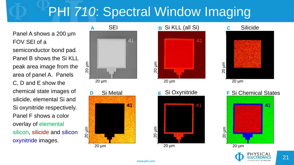
slide21. PHI 710: Spectral Window Imaging Panel A shows a 200 µm FOV SEI of a semiconductor bond pad. Panel B shows the Si KLL peak area image from the area of panel A. Panels C, D and E show the chemical state images of silicide, elemental Si and Si oxynitride respectively. Panel F shows a color overlay of elemental silicon, silicide and silicon oxynitride images. 21<br>
slide22. PHI 710: Thin Film Analysis World’s best Auger sputter depth profiling
Floating column ion gun for high current, low voltage sputter depth profiling
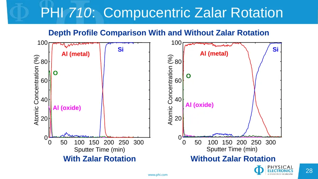
Compucentric Zalar Rotation™ minimizes sputtering artifacts and maximizes depth resolution
Image registration maintains field-of-view 22<br>
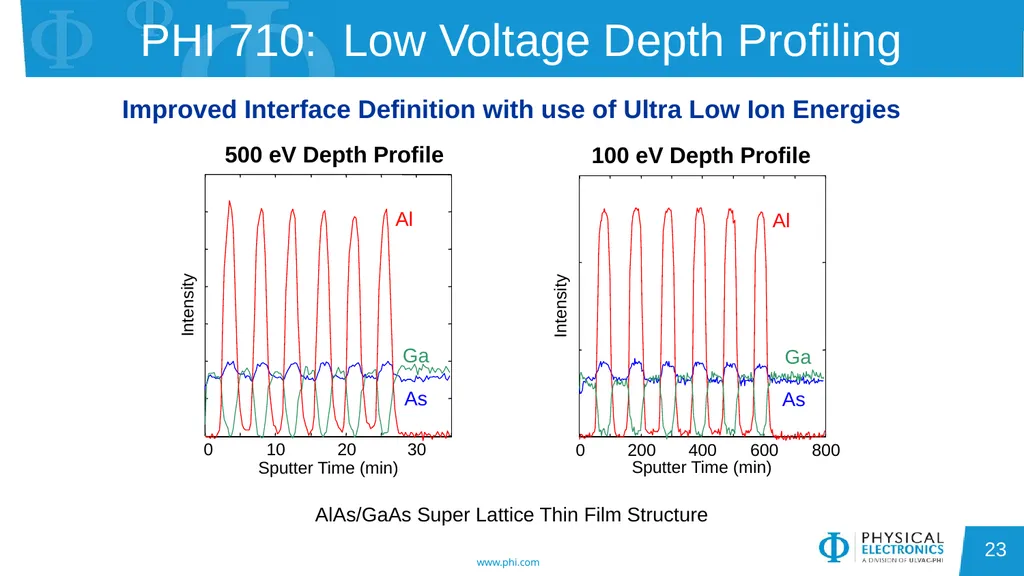
slide23. PHI 710: Low Voltage Depth Profiling Improved Interface Definition with use of Ultra Low Ion Energies AlAs/GaAs Super Lattice Thin Film Structure 23<br>
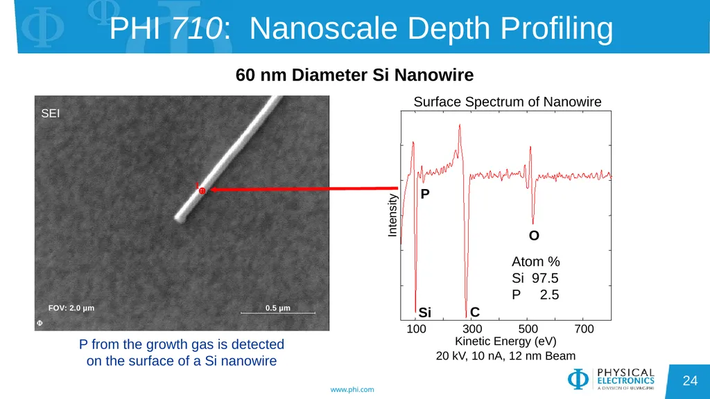
slide24. PHI 710: Nanoscale Depth Profiling P from the growth gas is detected on the surface of a Si nanowire 60 nm Diameter Si Nanowire 20 kV, 10 nA, 12 nm Beam 100 300 500 700 Kinetic Energy (eV) Intensity O C Si P Surface Spectrum of Nanowire SEI Atom %
Si 97.5
P 2.5 24<br>
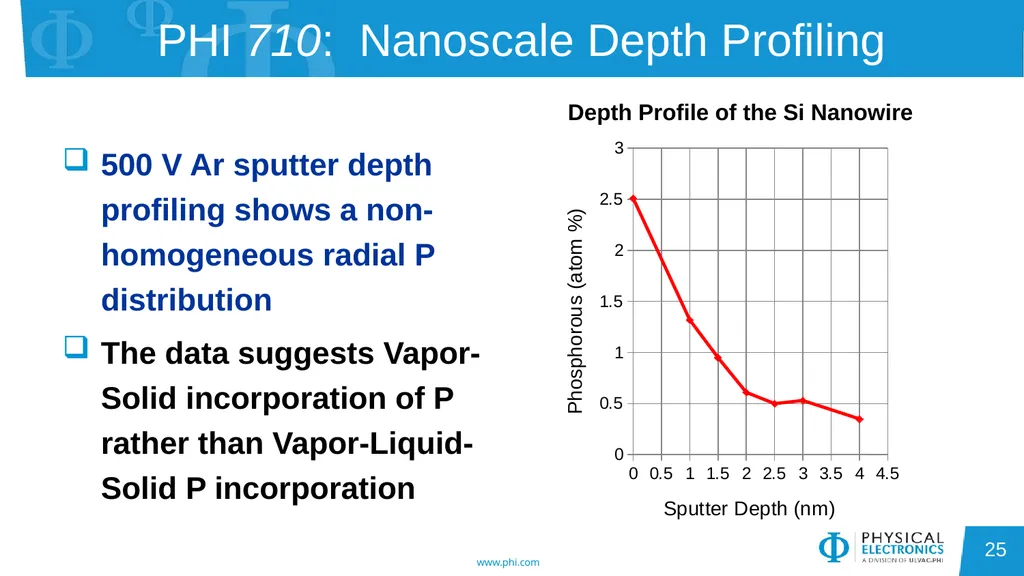
slide25. PHI 710: Nanoscale Depth Profiling 500 V Ar sputter depth profiling shows a non-homogeneous radial P distribution
The data suggests Vapor-Solid incorporation of P rather than Vapor-Liquid-Solid P incorporation Depth Profile of the Si Nanowire 25<br>
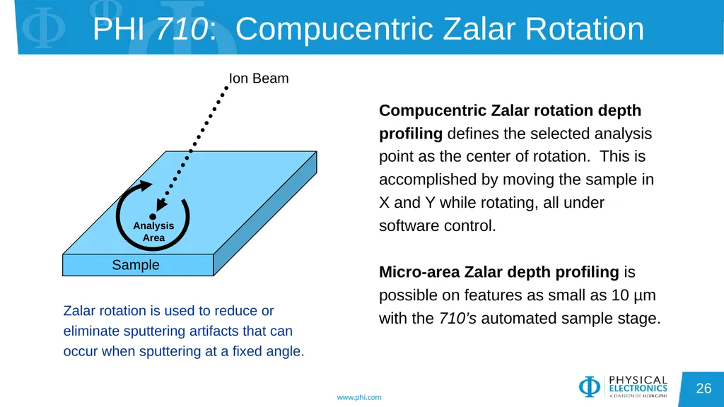
slide26. PHI 710: Compucentric Zalar Rotation Ion Beam Sample Analysis
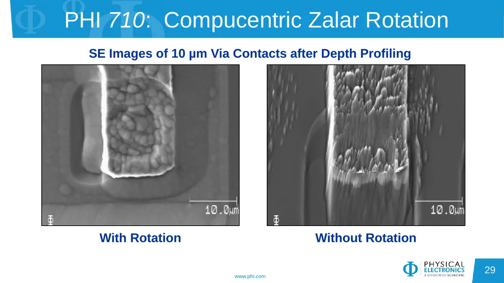
Area Zalar rotation is used to reduce or eliminate sputtering artifacts that can occur when sputtering at a fixed angle. Compucentric Zalar rotation depth profiling defines the selected analysis point as the center of rotation. This is accomplished by moving the sample in X and Y while rotating, all under software control.
Micro-area Zalar depth profiling is possible on features as small as 10 µm with the 710’s automated sample stage. 26<br>
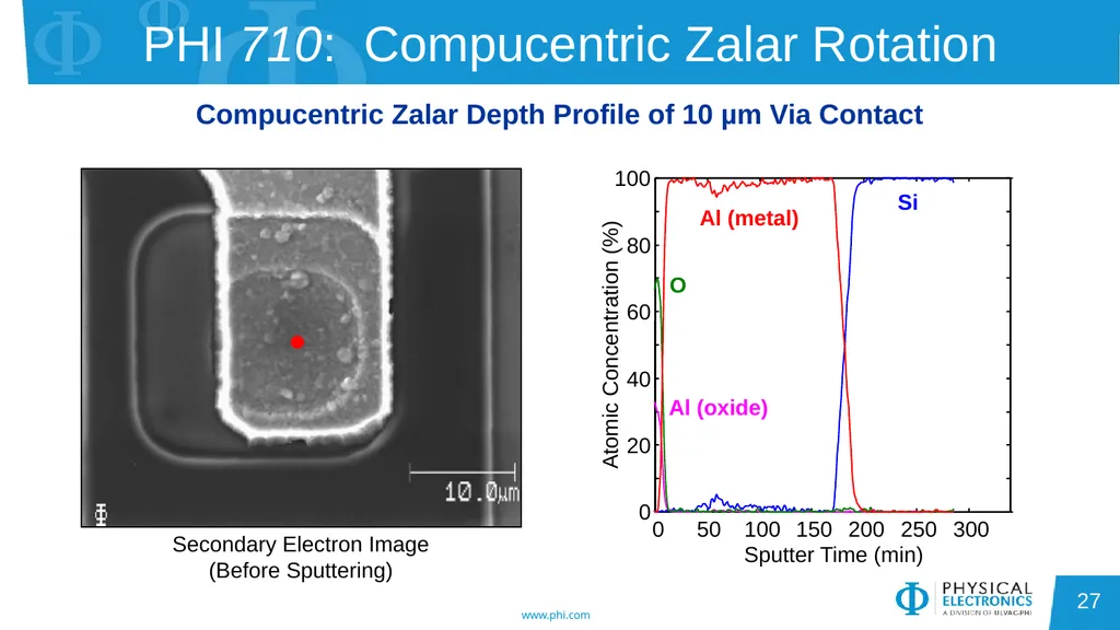
slide27. PHI 710: Compucentric Zalar Rotation Compucentric Zalar Depth Profile of 10 µm Via Contact Secondary Electron Image
(Before Sputtering) 27<br>
slide28. PHI 710: Compucentric Zalar Rotation Depth Profile Comparison With and Without Zalar Rotation Without Zalar Rotation With Zalar Rotation 28<br>
slide29. PHI 710: Compucentric Zalar Rotation Without Rotation With Rotation SE Images of 10 µm Via Contacts after Depth Profiling 29<br>
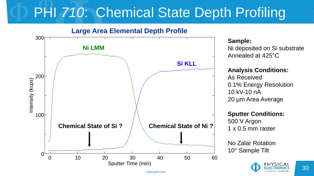
slide30. PHI 710: Chemical State Depth Profiling Sample:
Ni deposited on Si substrate
Annealed at 425°C
Analysis Conditions:
As Received
0.1% Energy Resolution
10 kV-10 nA
20 µm Area Average
Sputter Conditions:
500 V Argon
1 x 0.5 mm raster
No Zalar Rotation
10° Sample Tilt Large Area Elemental Depth Profile 30<br>
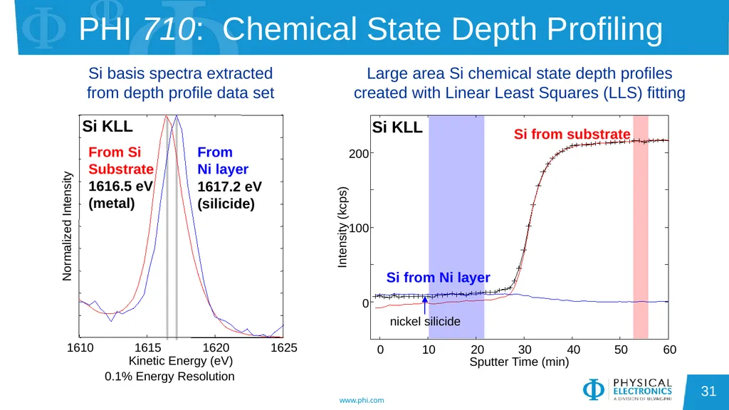
slide31. PHI 710: Chemical State Depth Profiling Si from Ni layer Si from substrate 0 10 20 30 40 50 60 0 100 200 Sputter Time (min) Intensity (kcps) Si KLL From
Ni layer
1617.2 eV
(silicide) From Si
Substrate
1616.5 eV
(metal) 1610 1615 1620 1625 Kinetic Energy (eV) Normalized Intensity Si KLL Large area Si chemical state depth profiles
created with Linear Least Squares (LLS) fitting 0.1% Energy Resolution Si basis spectra extracted from depth profile data set nickel silicide 31<br>
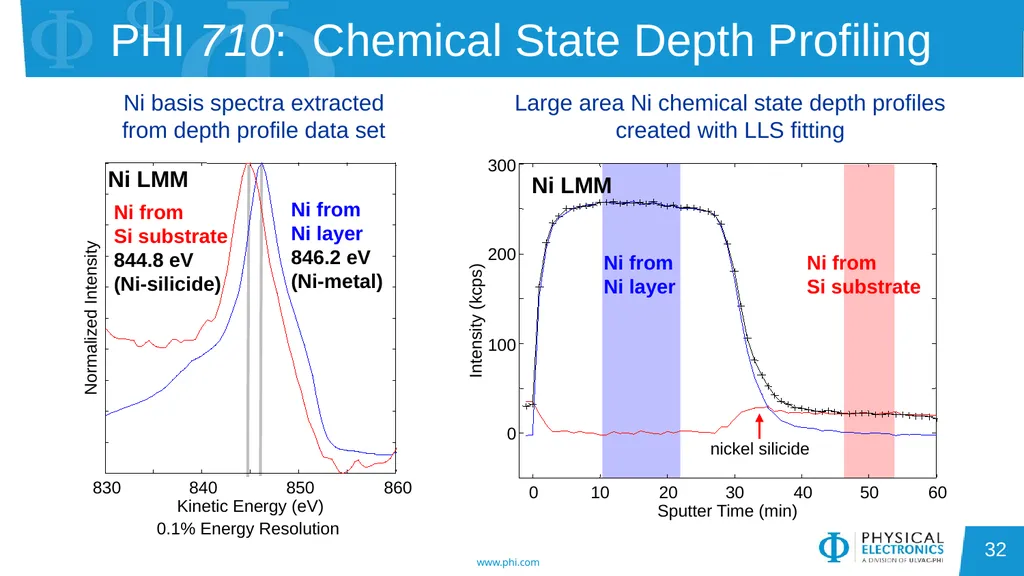
slide32. PHI 710: Chemical State Depth Profiling 0.1% Energy Resolution Ni from
Ni layer Ni from
Si substrate 0 10 20 30 40 50 60 0 100 200 300 Sputter Time (min) Intensity (kcps) Ni LMM Ni from
Ni layer
846.2 eV
(Ni-metal) Ni from
Si substrate
844.8 eV
(Ni-silicide) 830 840 850 860 Kinetic Energy (eV) Normalized Intensity Ni LMM Large area Ni chemical state depth profiles
created with LLS fitting Ni basis spectra extracted from depth profile data set nickel silicide 32<br>
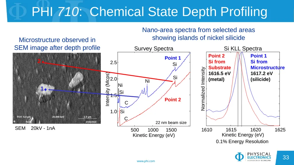
slide33. PHI 710: Chemical State Depth Profiling 1 2 SEM 20kV - 1nA 500 1000 1500 1.0 1.5 2.0 2.5 Kinetic Energy (eV) Intensity (Mcps) Si Ni Si Si Si C C Ni Point 1 Point 2 22 nm beam size Point 2
Si from
Substrate
1616.5 eV
(metal) Point 1
Si from
Microstructure
1617.2 eV
(silicide) 1610 1615 1620 1625 Kinetic Energy (eV) Normalized Intensity Si KLL Spectra Microstructure observed in SEM image after depth profile Survey Spectra 0.1% Energy Resolution Nano-area spectra from selected areas showing islands of nickel silicide 33<br>
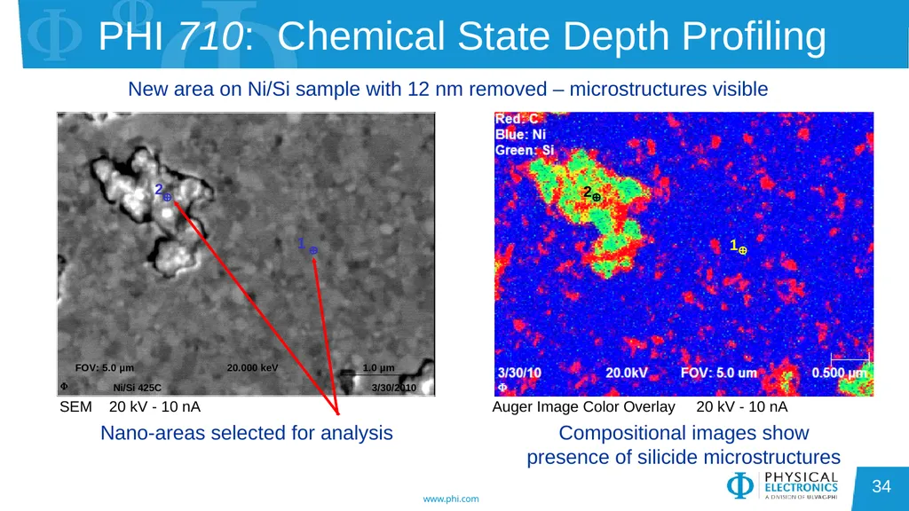
slide34. PHI 710: Chemical State Depth Profiling 1 2 SEM 20 kV - 10 nA Auger Image Color Overlay 20 kV - 10 nA New area on Ni/Si sample with 12 nm removed – microstructures visible Nano-areas selected for analysis Compositional images show presence of silicide microstructures 34<br>
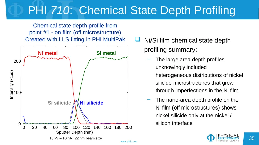
slide35. PHI 710: Chemical State Depth Profiling Ni/Si film chemical state depth profiling summary:
The large area depth profiles unknowingly included heterogeneous distributions of nickel silicide microstructures that grew through imperfections in the Ni film
The nano-area depth profile on the Ni film (off microstructures) shows nickel silicide only at the nickel / silicon interface Chemical state depth profile from
point #1 - on film (off microstructure)
Created with LLS fitting in PHI MultiPak 0 20 40 60 80 100 120 140 160 180 200 0 100 200 Sputter Depth (nm) Intensity (kcps) Si metal Si silicide Ni metal Ni silicide 10 kV – 10 nA 22 nm beam size 35<br>
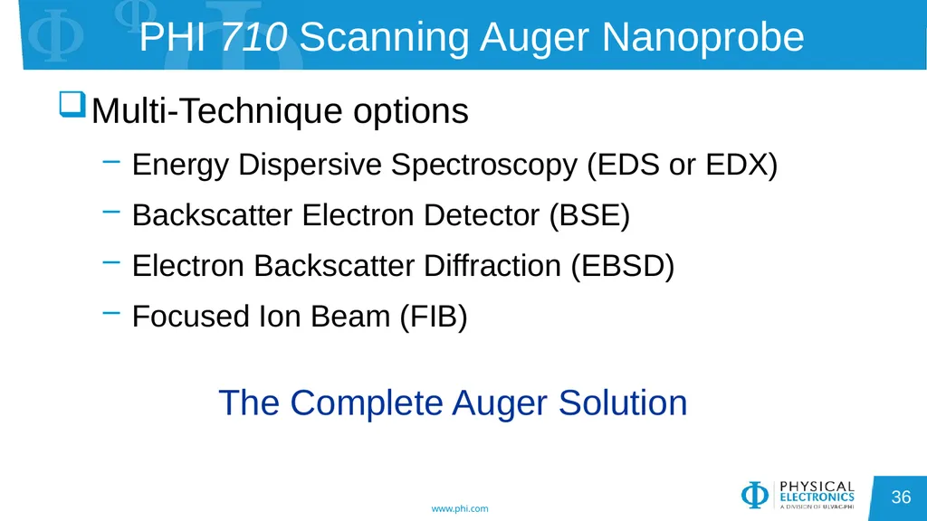
slide36. PHI 710 Scanning Auger Nanoprobe Multi-Technique options
Energy Dispersive Spectroscopy (EDS or EDX)
Backscatter Electron Detector (BSE)
Electron Backscatter Diffraction (EBSD)
Focused Ion Beam (FIB) The Complete Auger Solution 36<br>
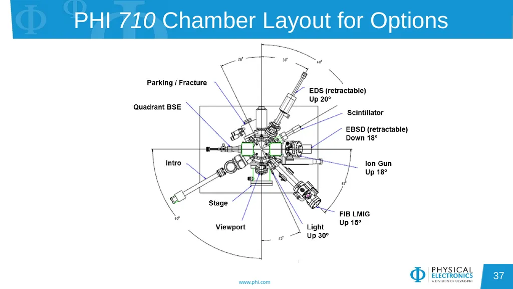
slide37. PHI 710 Chamber Layout for Options 37<br>
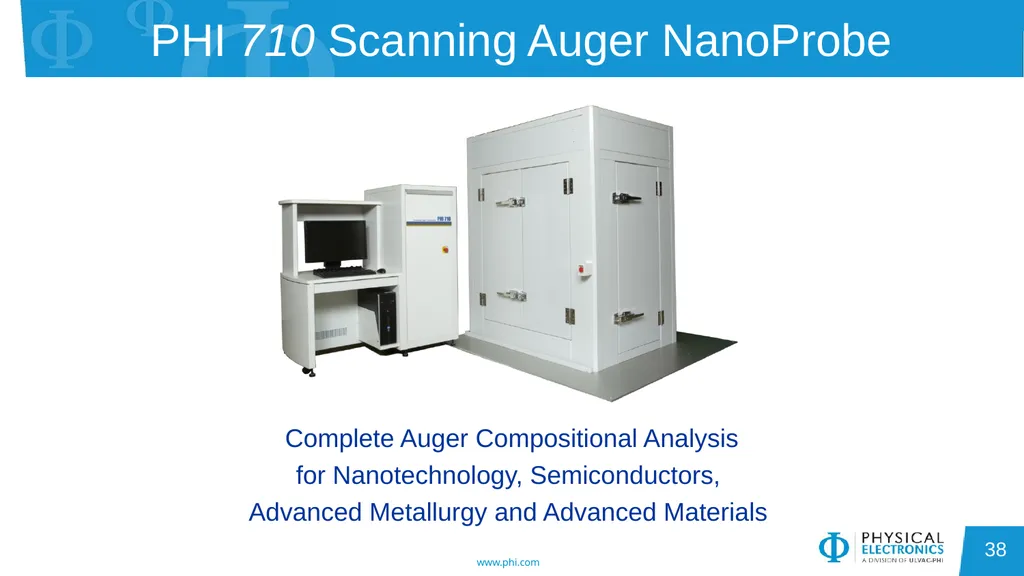
slide38. PHI 710 Scanning Auger NanoProbe Complete Auger Compositional Analysis
for Nanotechnology, Semiconductors,
Advanced Metallurgy and Advanced Materials 38<br>
slide2. Auger Electron Spectroscopy EKLL = EK - EL - EL’ AES Spectra of Cu Note that Auger peaks are typically superimposed on a large background (see red and magenta spectra).
For this reason Auger spectra are typically displayed in a differentiated mode as shown in the green spectrum.
Detection limits for AES are approximately 0.1 atomic percent. 2<br>
slide3. Auger Electron and X-ray Emission Incident
Beam Auger Electron X-ray
Photon Energy Dispersive X-ray Spectroscopy (EDX) Auger Electron Emission Incident Beam Incident Beam Auger Electron X-ray 3<br>
slide4. AES and EDX AES Provides Superior Nanovolume Analysis Capabilities EDX minimum analysis area > 1 µm 710 AES minimum analysis area 8 nm 4<br>
slide5. AES Analysis Depth Mean Free Path: Mean distance electrons travel before undergoing inelastic scattering 5<br>
slide6. Analysis Depth – “Universal” Curve 6<br>
slide7. Auger Electron Spectroscopy Auger Electron Spectroscopy is an analytical technique that provides compositional information from the top few monolayers of a material
Detect all elements above He
Detection limits: 0.1 – 1 atomic %
Surface sensitive: top 5-75 Å
Spatial resolution: < 60 Å probe size (PHI 710) 7<br>
slide8. What Information Does Auger Provide ? Surface composition at high spatial resolution
Secondary Electron Imaging
Provides high magnification visualization of the sample
Elemental analysis (spectra)
Determines what elements are present & their quantity
Elemental imaging (mapping)
Illustrates two-dimensional elemental distributions
High energy resolution spectra, imaging and depth profiling
Chemical state analysis for some materials
Sputter depth profiling
Reveals thin film and interfacial composition 8<br>
slide9. PHI 710 Scanning Auger NanoProbe 9<br>
slide10. PHI 710: Analytical Capabilities Nanoscale image resolution
Image registration for high sensitivity
Constant sensitivity for all geometries
Constant sensitivity with tilt for insulators
Nano-volume depth profiling
Chemical state analysis 10<br>
slide11. PHI 710: High Spatial Resolution Locations for Line Scans Area Analyzed 4 nm Al Line AlGaAs Line Width (nm) Auger
Line
Scans Sample provided by Federal Institute for Materials Research and Testing (BAM)
Berlin, Germany 24 hour stability test demonstrating exceptional image registry BAM-L200 Standard Sample Ga Map 25 kV - 1 nA 256x256 pixels Al Map 25 kV - 1 nA 256x256 pixels 11<br>
slide12. PHI 710: High Spatial Resolution 4 nm Al Line 0 0.05 0.10 0.15 0.20 0.25 0.30 0.35 Distance (µm) Intensity Ga Al (X3) BAM-L200 Standard Sample Line Scan #4 24 hour stability test demonstrating exceptional image registry 12<br>
slide13. PHI 710: Constant Sensitivity for All Geometries PHI 710
Coaxial Analyzer & Electron Gun Geometry The CMA with coaxial electron gun provides high sensitivity at all sample tilt angles which is essential for insulator analysis and samples with topography 13<br>
slide14. PHI 710: CMA with Coaxial Geometry Secondary Electron Image Ni Map In Map No shadowing
Every pixel can be identified as part of a Ni sphere or as part of the In substrate.
The Ni particles are complete spheres and the substrate fills in around the particles.
Variations in In and Ni intensity provide meaningful compositional information. 14<br>
slide15. Non-Coaxial Geometry Secondary Electron Image Ni Map In Map Shadowing
Many pixels are of unknown composition, apparently neither Ni balls nor In substrate.
The Ni particles are not observed as complete spheres and very little of the substrate is seen.
Variations in In and Ni intensity do not provide meaningful compositional information. 15<br>
slide16. PHI 710 High Energy Resolution Mode How does the high energy resolution mode work?
The CMA energy resolution is given as:
ΔE / E = 0.5%
An optics element placed between the sample surface and the entrance to the standard CMA retards the Auger electrons, reducing their energy, E
From the energy resolution equation, if E is reduced, ΔE is also reduced and so is the Auger peak width; energy resolution is improved
The CMA is not modified in any way and retains a 360º coaxial view of the sample relative to the axis of the electron gun
US Patent 12 / 705,261 16<br>
slide17. PHI 710 High Energy Resolution Mode 17<br>
slide18. PHI 710 High Energy Resolution Mode 1360 1370 1380 1390 1400 1410 -50 0 50 100 150 200 250 300 350 1393.4 eV (Al metal) (Al oxide) 1386.9 eV Kinetic Energy (eV) N(E) cps Al KLL Spectra of Native Oxide on Al Foil Energy
Resolution 0.5 % 0.1 % 18<br>
slide19. PHI 710 High Energy Resolution Mode Depth Profile of Zn Oxide on Zn 19<br>
slide20. PHI 710: Spectral Window Imaging B Panel A shows the Si KLL spectrum from the sum of all pixel spectra in the Si KLL Auger image shown in panel B. Panel B shows the three Regions Of Interest (ROI) selected for creation of the basis spectra for Linear Least Squares (LLS) fitting of the Si KLL image data set. Panel C shows the three basis spectra with their corresponding chemical state identifications. In the spectral window imaging mode, a Si KLL spectrum is collected and stored for each image pixel. 20<br>
slide21. PHI 710: Spectral Window Imaging Panel A shows a 200 µm FOV SEI of a semiconductor bond pad. Panel B shows the Si KLL peak area image from the area of panel A. Panels C, D and E show the chemical state images of silicide, elemental Si and Si oxynitride respectively. Panel F shows a color overlay of elemental silicon, silicide and silicon oxynitride images. 21<br>
slide22. PHI 710: Thin Film Analysis World’s best Auger sputter depth profiling
Floating column ion gun for high current, low voltage sputter depth profiling
Compucentric Zalar Rotation™ minimizes sputtering artifacts and maximizes depth resolution
Image registration maintains field-of-view 22<br>
slide23. PHI 710: Low Voltage Depth Profiling Improved Interface Definition with use of Ultra Low Ion Energies AlAs/GaAs Super Lattice Thin Film Structure 23<br>
slide24. PHI 710: Nanoscale Depth Profiling P from the growth gas is detected on the surface of a Si nanowire 60 nm Diameter Si Nanowire 20 kV, 10 nA, 12 nm Beam 100 300 500 700 Kinetic Energy (eV) Intensity O C Si P Surface Spectrum of Nanowire SEI Atom %
Si 97.5
P 2.5 24<br>
slide25. PHI 710: Nanoscale Depth Profiling 500 V Ar sputter depth profiling shows a non-homogeneous radial P distribution
The data suggests Vapor-Solid incorporation of P rather than Vapor-Liquid-Solid P incorporation Depth Profile of the Si Nanowire 25<br>
slide26. PHI 710: Compucentric Zalar Rotation Ion Beam Sample Analysis
Area Zalar rotation is used to reduce or eliminate sputtering artifacts that can occur when sputtering at a fixed angle. Compucentric Zalar rotation depth profiling defines the selected analysis point as the center of rotation. This is accomplished by moving the sample in X and Y while rotating, all under software control.
Micro-area Zalar depth profiling is possible on features as small as 10 µm with the 710’s automated sample stage. 26<br>
slide27. PHI 710: Compucentric Zalar Rotation Compucentric Zalar Depth Profile of 10 µm Via Contact Secondary Electron Image
(Before Sputtering) 27<br>
slide28. PHI 710: Compucentric Zalar Rotation Depth Profile Comparison With and Without Zalar Rotation Without Zalar Rotation With Zalar Rotation 28<br>
slide29. PHI 710: Compucentric Zalar Rotation Without Rotation With Rotation SE Images of 10 µm Via Contacts after Depth Profiling 29<br>
slide30. PHI 710: Chemical State Depth Profiling Sample:
Ni deposited on Si substrate
Annealed at 425°C
Analysis Conditions:
As Received
0.1% Energy Resolution
10 kV-10 nA
20 µm Area Average
Sputter Conditions:
500 V Argon
1 x 0.5 mm raster
No Zalar Rotation
10° Sample Tilt Large Area Elemental Depth Profile 30<br>
slide31. PHI 710: Chemical State Depth Profiling Si from Ni layer Si from substrate 0 10 20 30 40 50 60 0 100 200 Sputter Time (min) Intensity (kcps) Si KLL From
Ni layer
1617.2 eV
(silicide) From Si
Substrate
1616.5 eV
(metal) 1610 1615 1620 1625 Kinetic Energy (eV) Normalized Intensity Si KLL Large area Si chemical state depth profiles
created with Linear Least Squares (LLS) fitting 0.1% Energy Resolution Si basis spectra extracted from depth profile data set nickel silicide 31<br>
slide32. PHI 710: Chemical State Depth Profiling 0.1% Energy Resolution Ni from
Ni layer Ni from
Si substrate 0 10 20 30 40 50 60 0 100 200 300 Sputter Time (min) Intensity (kcps) Ni LMM Ni from
Ni layer
846.2 eV
(Ni-metal) Ni from
Si substrate
844.8 eV
(Ni-silicide) 830 840 850 860 Kinetic Energy (eV) Normalized Intensity Ni LMM Large area Ni chemical state depth profiles
created with LLS fitting Ni basis spectra extracted from depth profile data set nickel silicide 32<br>
slide33. PHI 710: Chemical State Depth Profiling 1 2 SEM 20kV - 1nA 500 1000 1500 1.0 1.5 2.0 2.5 Kinetic Energy (eV) Intensity (Mcps) Si Ni Si Si Si C C Ni Point 1 Point 2 22 nm beam size Point 2
Si from
Substrate
1616.5 eV
(metal) Point 1
Si from
Microstructure
1617.2 eV
(silicide) 1610 1615 1620 1625 Kinetic Energy (eV) Normalized Intensity Si KLL Spectra Microstructure observed in SEM image after depth profile Survey Spectra 0.1% Energy Resolution Nano-area spectra from selected areas showing islands of nickel silicide 33<br>
slide34. PHI 710: Chemical State Depth Profiling 1 2 SEM 20 kV - 10 nA Auger Image Color Overlay 20 kV - 10 nA New area on Ni/Si sample with 12 nm removed – microstructures visible Nano-areas selected for analysis Compositional images show presence of silicide microstructures 34<br>
slide35. PHI 710: Chemical State Depth Profiling Ni/Si film chemical state depth profiling summary:
The large area depth profiles unknowingly included heterogeneous distributions of nickel silicide microstructures that grew through imperfections in the Ni film
The nano-area depth profile on the Ni film (off microstructures) shows nickel silicide only at the nickel / silicon interface Chemical state depth profile from
point #1 - on film (off microstructure)
Created with LLS fitting in PHI MultiPak 0 20 40 60 80 100 120 140 160 180 200 0 100 200 Sputter Depth (nm) Intensity (kcps) Si metal Si silicide Ni metal Ni silicide 10 kV – 10 nA 22 nm beam size 35<br>
slide36. PHI 710 Scanning Auger Nanoprobe Multi-Technique options
Energy Dispersive Spectroscopy (EDS or EDX)
Backscatter Electron Detector (BSE)
Electron Backscatter Diffraction (EBSD)
Focused Ion Beam (FIB) The Complete Auger Solution 36<br>
slide37. PHI 710 Chamber Layout for Options 37<br>
slide38. PHI 710 Scanning Auger NanoProbe Complete Auger Compositional Analysis
for Nanotechnology, Semiconductors,
Advanced Metallurgy and Advanced Materials 38<br>