Buck Regulator Architectures 4.4 Constant On Time (COT) Buck Regulators Constant ON-Time (COT) Hysteretic Regulator Advantages Constant frequency vs. VIN High Efficiency at light load Fast transient response Disadvantages Requires ripple at
"Buck Regulator Architectures 4.4 Constant On Time" is the property of its rightful owner. Permission is granted to
download and print the materials on this website for personal, non-commercial use only, and to display it
on your personal computer provided you do not modify the materials and that you retain all copyright
notices contained in the materials. By downloading content from our website, you accept the terms of this
agreement.
Presentation Transcript
01
Buck Regulator Architectures 4.4 Constant On Time (COT) Buck Regulators<br>
02
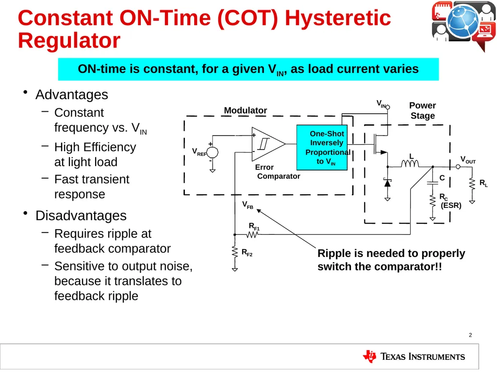
Constant ON-Time (COT) Hysteretic Regulator Advantages
Constant frequency vs. VIN
High Efficiency at light load
Fast transient response
Disadvantages
Requires ripple at feedback comparator
Sensitive to output noise, because it translates to feedback ripple 2 ON-time is constant, for a given VIN, as load current varies<br>
03
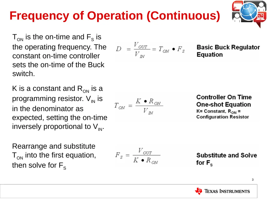
Frequency of Operation (Continuous) TON is the on-time and FS is the operating frequency. The constant on-time controller sets the on-time of the Buck switch. 3 K is a constant and RON is a programming resistor. VIN is in the denominator as expected, setting the on-time inversely proportional to VIN. Rearrange and substitute TON into the first equation, then solve for FS<br>
04
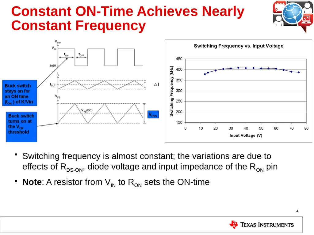
Constant ON-Time Achieves Nearly Constant Frequency Switching frequency is almost constant; the variations are due to effects of RDS-ON, diode voltage and input impedance of the RON pin
Note: A resistor from VIN to RON sets the ON-time 4<br>
05
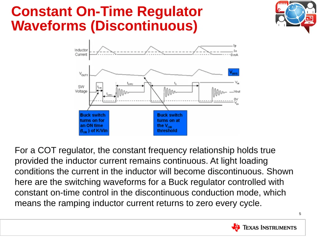
Constant On-Time Regulator Waveforms (Discontinuous) For a COT regulator, the constant frequency relationship holds true provided the inductor current remains continuous. At light loading conditions the current in the inductor will become discontinuous. Shown here are the switching waveforms for a Buck regulator controlled with constant on-time control in the discontinuous conduction mode, which means the ramping inductor current returns to zero every cycle. 5<br>
06
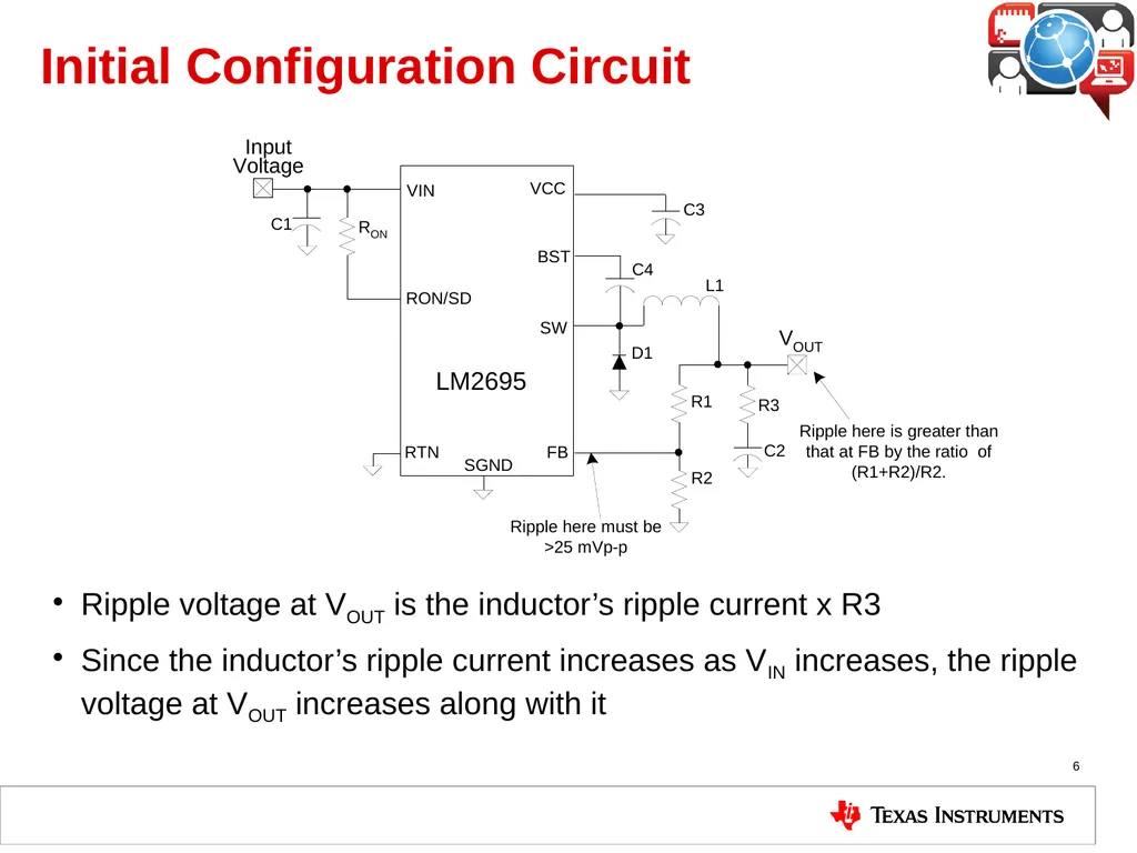
Initial Configuration Circuit Ripple voltage at VOUT is the inductor’s ripple current x R3
Since the inductor’s ripple current increases as VIN increases, the ripple voltage at VOUT increases along with it 6<br>
07
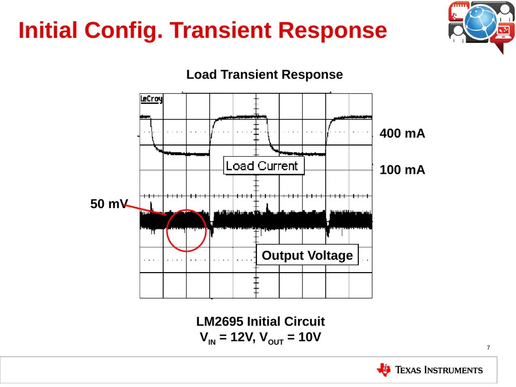
Initial Config. Transient Response 7<br>
08
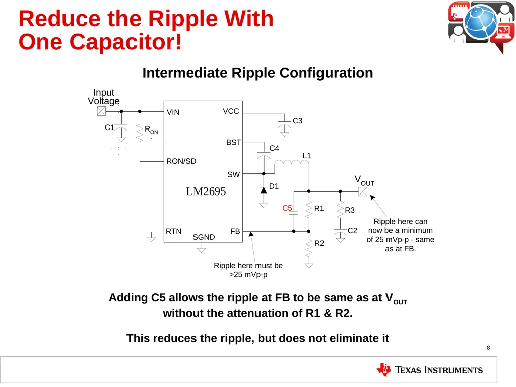
Reduce the Ripple With One Capacitor! 8 Adding C5 allows the ripple at FB to be same as at VOUT without the attenuation of R1 & R2. This reduces the ripple, but does not eliminate it Intermediate Ripple Configuration<br>
09
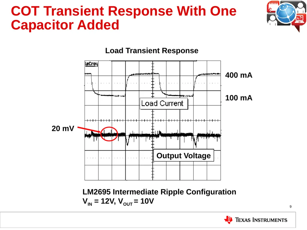
COT Transient Response With One Capacitor Added 9 LM2695 Intermediate Ripple Configuration
VIN = 12V, VOUT = 10V 400 mA 100 mA Output Voltage 20 mV Load Transient Response<br>
10
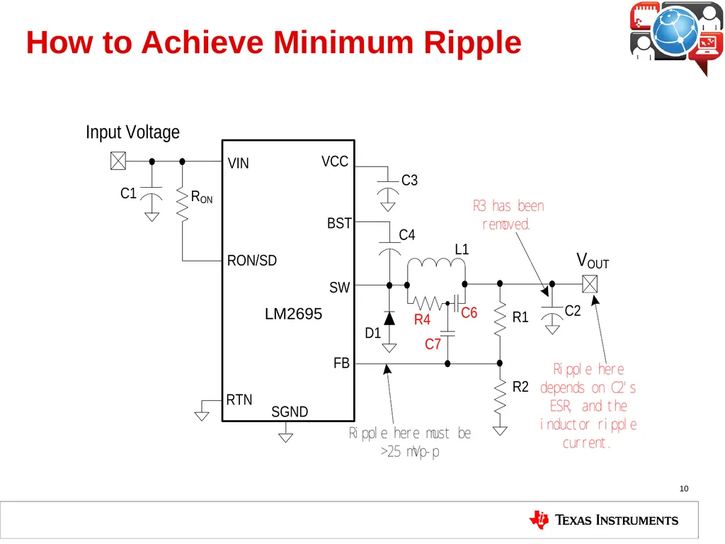
How to Achieve Minimum Ripple 10<br>
11
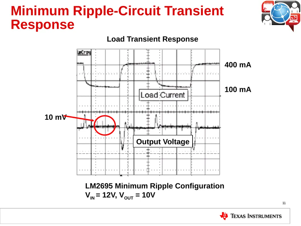
Minimum Ripple-Circuit Transient Response 11 LM2695 Minimum Ripple Configuration
VIN = 12V, VOUT = 10V Load Transient Response Output Voltage 400 mA 100 mA 10 mV<br>
12
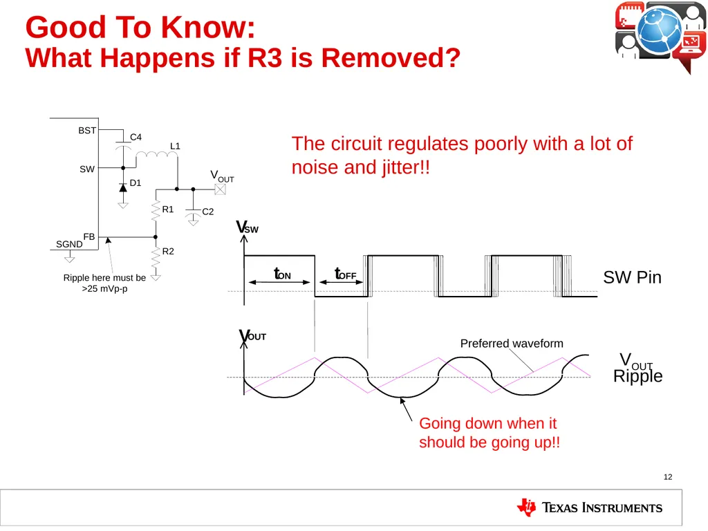
Good To Know: What Happens if R3 is Removed? 12 Going down when it should be going up!! The circuit regulates poorly with a lot of noise and jitter!!<br>
13
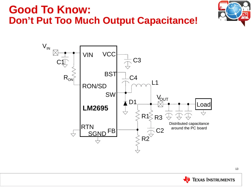
Good To Know: Don’t Put Too Much Output Capacitance! 13<br>
14
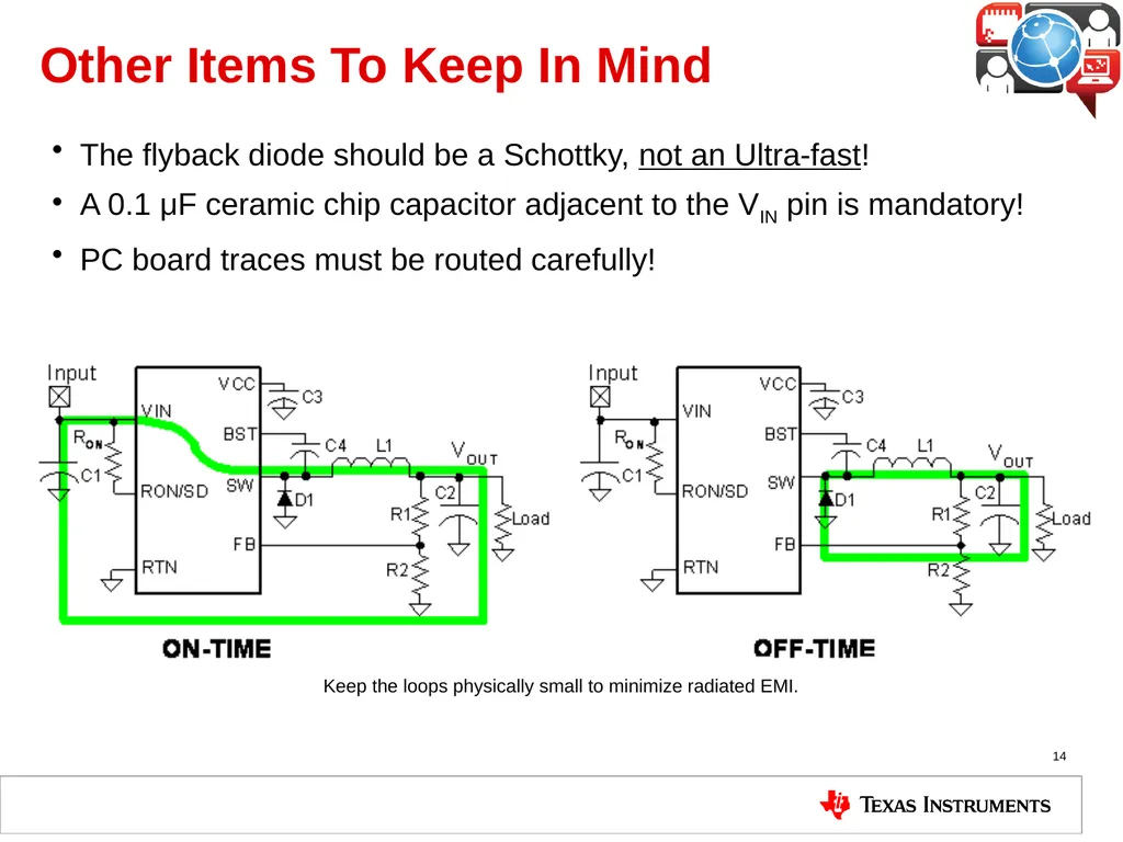
Other Items To Keep In Mind The flyback diode should be a Schottky, not an Ultra-fast!
A 0.1 μF ceramic chip capacitor adjacent to the VIN pin is mandatory!
PC board traces must be routed carefully! 14 Keep the loops physically small to minimize radiated EMI.<br>