
CSE 140: Components and Design Techniques for
CS
Published · 46 slides · 0 views
1 / 1

Description
CSE 140: Components and Design Techniques for Digital Systems Lecture 10: Sequential Networks: Timing and Retiming CK Cheng Dept. of Computer Science and Engineering University of California, San Diego 1 Timing Motivation Gate Delay
Related Topics
Share
Embed code
Download this presentation From Below
"CSE 140: Components and Design Techniques for" is the property of its rightful owner. Permission is granted to download and print the materials on this website for personal, non-commercial use only, and to display it on your personal computer provided you do not modify the materials and that you retain all copyright notices contained in the materials. By downloading content from our website, you accept the terms of this agreement.
Presentation Transcript
01
CSE 140: Components and Design Techniques for Digital Systems
Lecture 10:
Sequential Networks: Timing and Retiming
CK Cheng
Dept. of Computer Science and Engineering
University of California, San Diego 1<br>
Lecture 10:
Sequential Networks: Timing and Retiming
CK Cheng
Dept. of Computer Science and Engineering
University of California, San Diego 1<br>
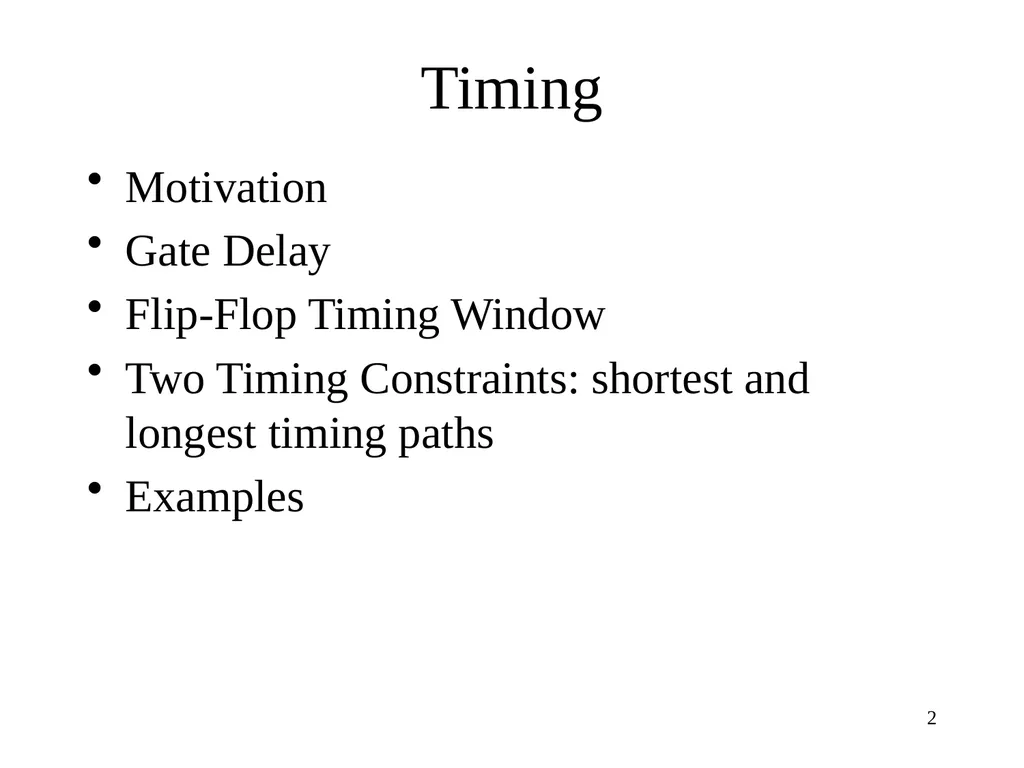
02
Timing Motivation
Gate Delay
Flip-Flop Timing Window
Two Timing Constraints: shortest and longest timing paths
Examples 2<br>
Gate Delay
Flip-Flop Timing Window
Two Timing Constraints: shortest and longest timing paths
Examples 2<br>
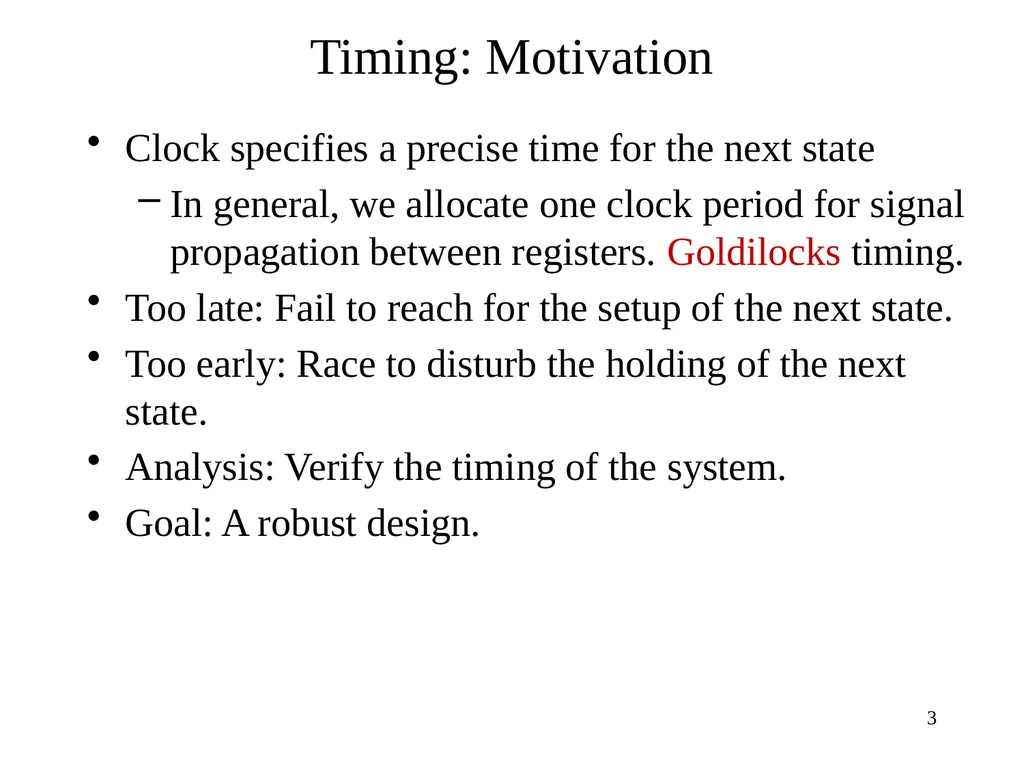
03
Timing: Motivation Clock specifies a precise time for the next state
In general, we allocate one clock period for signal propagation between registers. Goldilocks timing.
Too late: Fail to reach for the setup of the next state.
Too early: Race to disturb the holding of the next state.
Analysis: Verify the timing of the system.
Goal: A robust design. 3<br>
In general, we allocate one clock period for signal propagation between registers. Goldilocks timing.
Too late: Fail to reach for the setup of the next state.
Too early: Race to disturb the holding of the next state.
Analysis: Verify the timing of the system.
Goal: A robust design. 3<br>
04
The Story of Goldilocks and the Three Bears Once upon a time, there was a little girl named Goldilocks. She went for a walk in the forest. Pretty soon, she came upon a house. She knocked and, when no one answered, she walked right in. At the table in the kitchen, there were three bowls of porridge. Goldilocks was hungry. She tasted the porridge from the first bowl. "This porridge is too hot!" she exclaimed. So, she tasted the porridge from the second bowl.
"This porridge is too cold," she said. So, she tasted the last bowl of porridge. "Ahhh, this porridge is just right," she said happily and
she ate it all up. DLTK's Crafts for Kids 4<br>
"This porridge is too cold," she said. So, she tasted the last bowl of porridge. "Ahhh, this porridge is just right," she said happily and
she ate it all up. DLTK's Crafts for Kids 4<br>
05
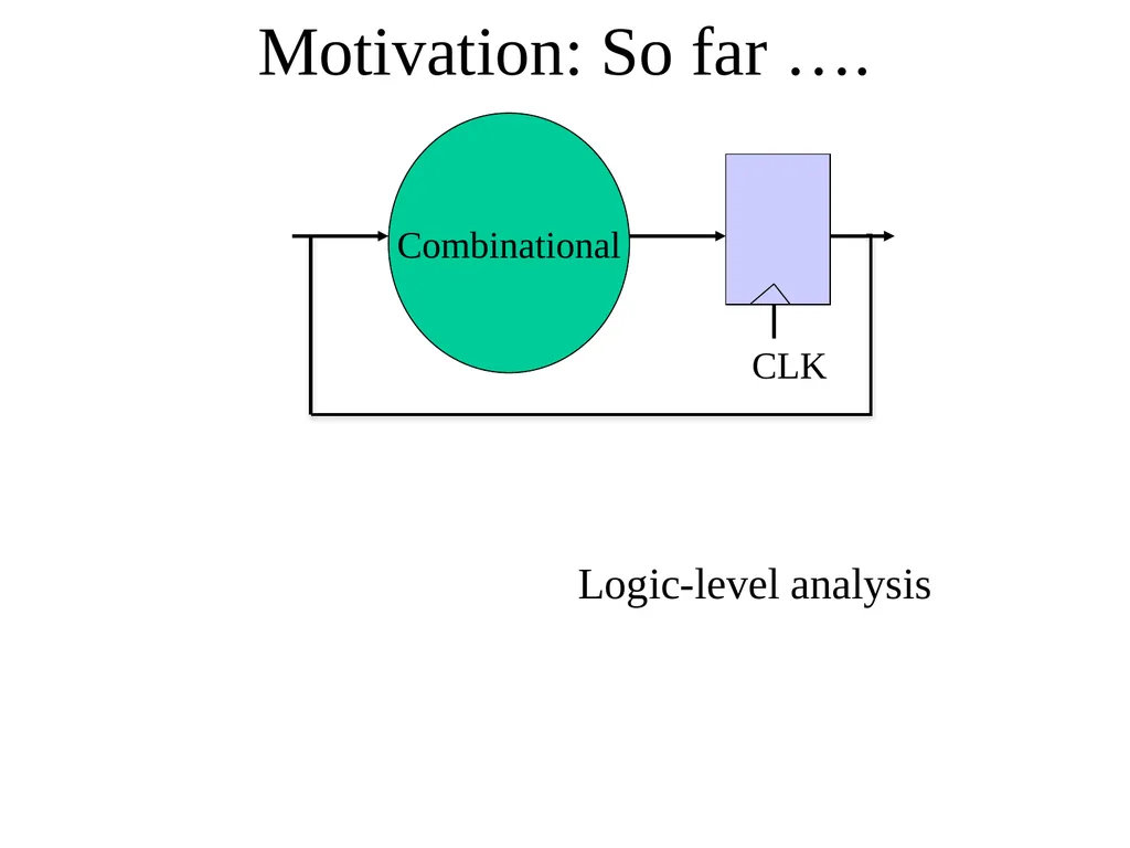
Motivation: So far …. Logic-level analysis<br>
06
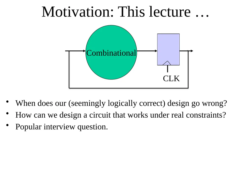
Motivation: This lecture … When does our (seemingly logically correct) design go wrong?
How can we design a circuit that works under real constraints?
Popular interview question.<br>
How can we design a circuit that works under real constraints?
Popular interview question.<br>
07
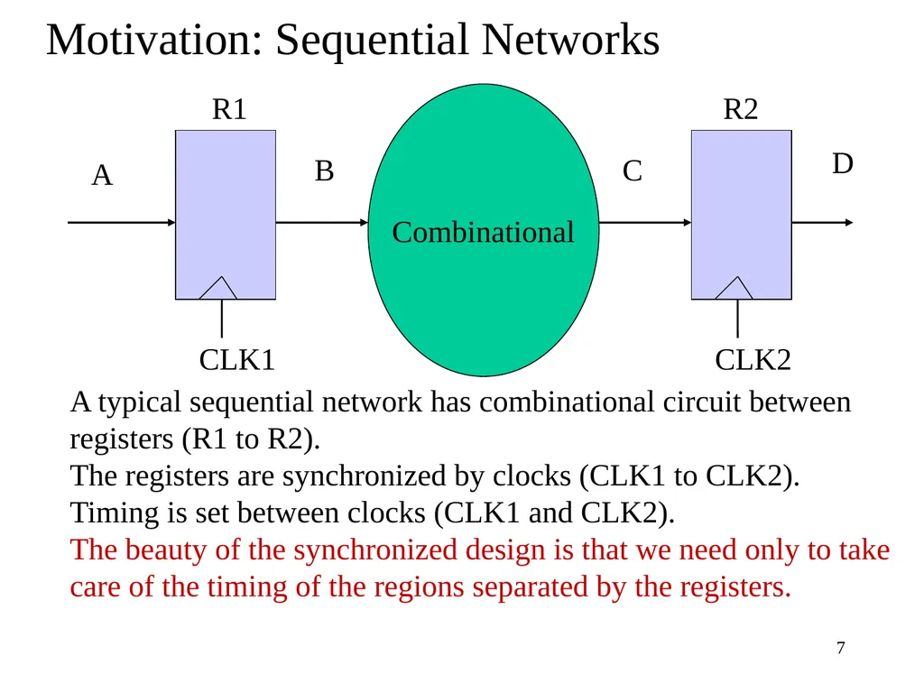
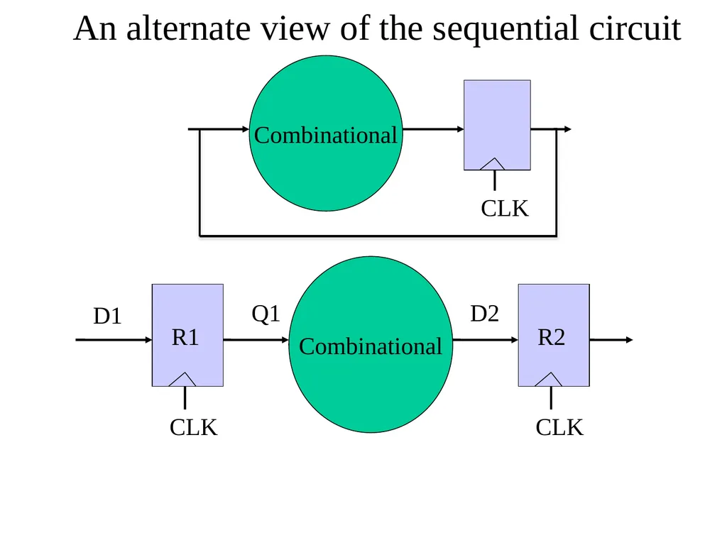
A typical sequential network has combinational circuit between registers (R1 to R2).
The registers are synchronized by clocks (CLK1 to CLK2).
Timing is set between clocks (CLK1 and CLK2).
The beauty of the synchronized design is that we need only to take care of the timing of the regions separated by the registers. Motivation: Sequential Networks 7<br>
The registers are synchronized by clocks (CLK1 to CLK2).
Timing is set between clocks (CLK1 and CLK2).
The beauty of the synchronized design is that we need only to take care of the timing of the regions separated by the registers. Motivation: Sequential Networks 7<br>
08
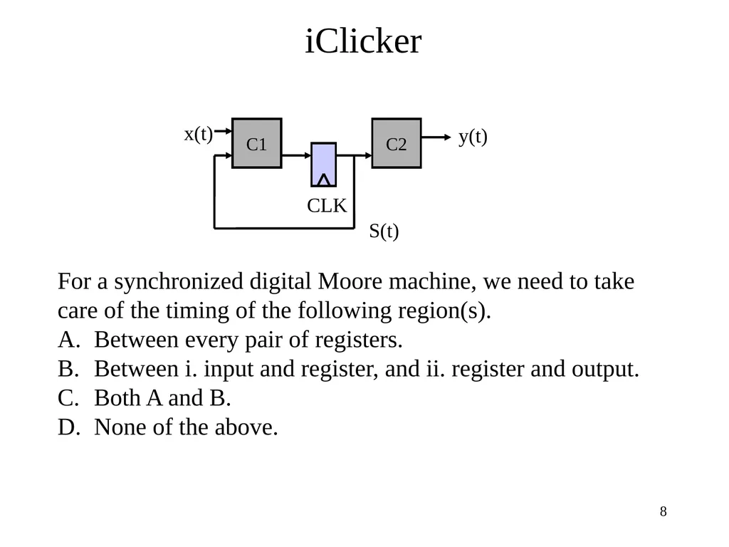
iClicker 8 For a synchronized digital Moore machine, we need to take care of the timing of the following region(s).
Between every pair of registers.
Between i. input and register, and ii. register and output.
Both A and B.
None of the above.<br>
Between every pair of registers.
Between i. input and register, and ii. register and output.
Both A and B.
None of the above.<br>
09
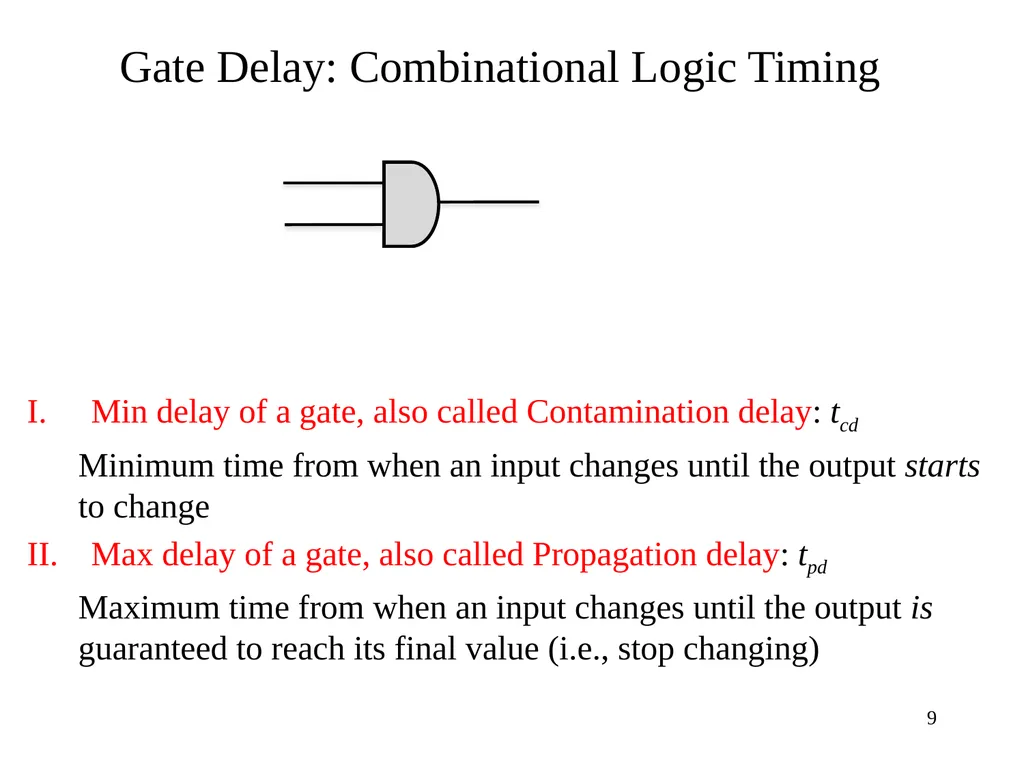
Gate Delay: Combinational Logic Timing 9 Min delay of a gate, also called Contamination delay: tcd
Minimum time from when an input changes until the output starts to change
Max delay of a gate, also called Propagation delay: tpd
Maximum time from when an input changes until the output is guaranteed to reach its final value (i.e., stop changing)<br>
Minimum time from when an input changes until the output starts to change
Max delay of a gate, also called Propagation delay: tpd
Maximum time from when an input changes until the output is guaranteed to reach its final value (i.e., stop changing)<br>
10
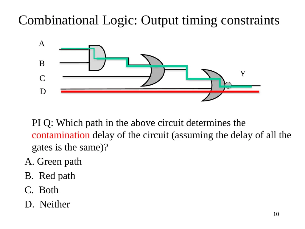
Combinational Logic: Output timing constraints 10 A B C D Y PI Q: Which path in the above circuit determines the contamination delay of the circuit (assuming the delay of all the gates is the same)?
Green path
Red path
Both
Neither<br>
Green path
Red path
Both
Neither<br>
11
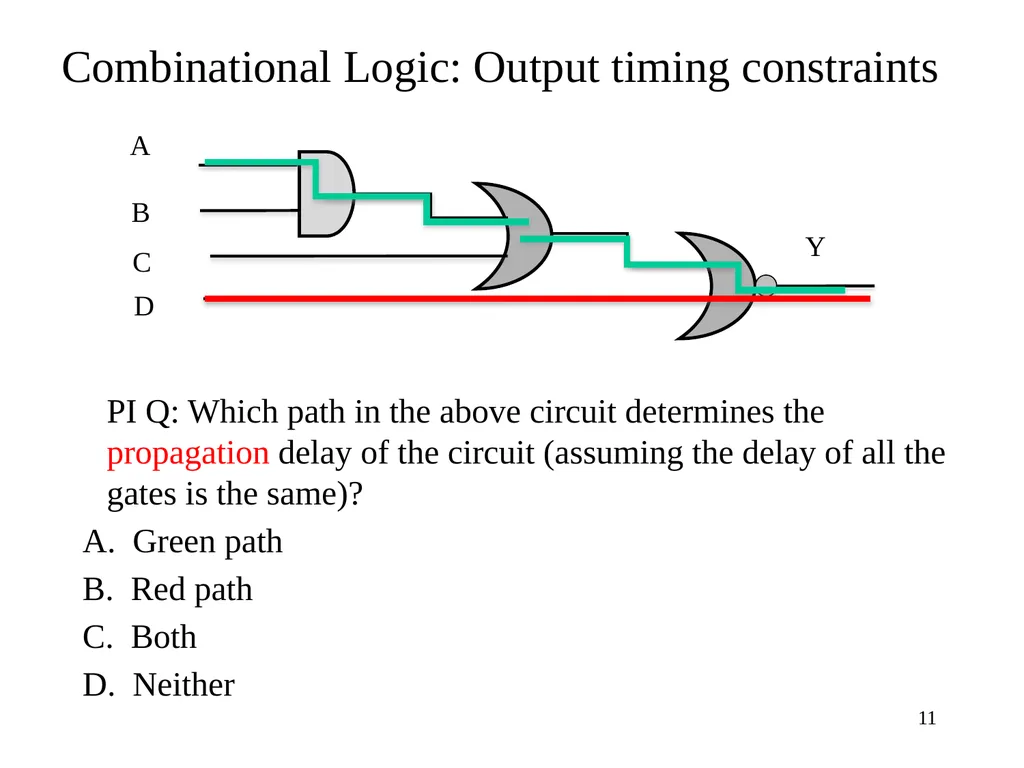
Combinational Logic: Output timing constraints 11 A B C D Y PI Q: Which path in the above circuit determines the propagation delay of the circuit (assuming the delay of all the gates is the same)?
Green path
Red path
Both
Neither<br>
Green path
Red path
Both
Neither<br>
12
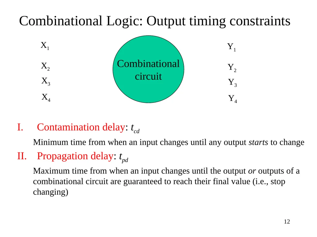
Combinational Logic: Output timing constraints 12 X1 X2 X4 Contamination delay: tcd
Minimum time from when an input changes until any output starts to change
Propagation delay: tpd
Maximum time from when an input changes until the output or outputs of a combinational circuit are guaranteed to reach their final value (i.e., stop changing) Combinational
circuit X3 Y1 Y2 Y4 Y3<br>
Minimum time from when an input changes until any output starts to change
Propagation delay: tpd
Maximum time from when an input changes until the output or outputs of a combinational circuit are guaranteed to reach their final value (i.e., stop changing) Combinational
circuit X3 Y1 Y2 Y4 Y3<br>
13
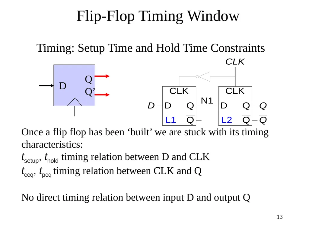
Flip-Flop Timing Window Timing: Setup Time and Hold Time Constraints 13 Once a flip flop has been ‘built’ we are stuck with its timing characteristics:
tsetup, thold timing relation between D and CLK
tccq, tpcq timing relation between CLK and Q
No direct timing relation between input D and output Q<br>
tsetup, thold timing relation between D and CLK
tccq, tpcq timing relation between CLK and Q
No direct timing relation between input D and output Q<br>
14
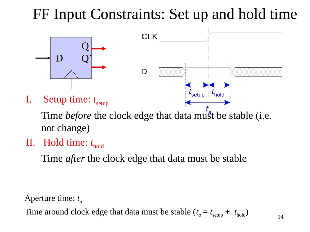
FF Input Constraints: Set up and hold time 14 Setup time: tsetup
Time before the clock edge that data must be stable (i.e. not change)
Hold time: thold
Time after the clock edge that data must be stable Aperture time: ta
Time around clock edge that data must be stable (ta = tsetup + thold)<br>
Time before the clock edge that data must be stable (i.e. not change)
Hold time: thold
Time after the clock edge that data must be stable Aperture time: ta
Time around clock edge that data must be stable (ta = tsetup + thold)<br>
15
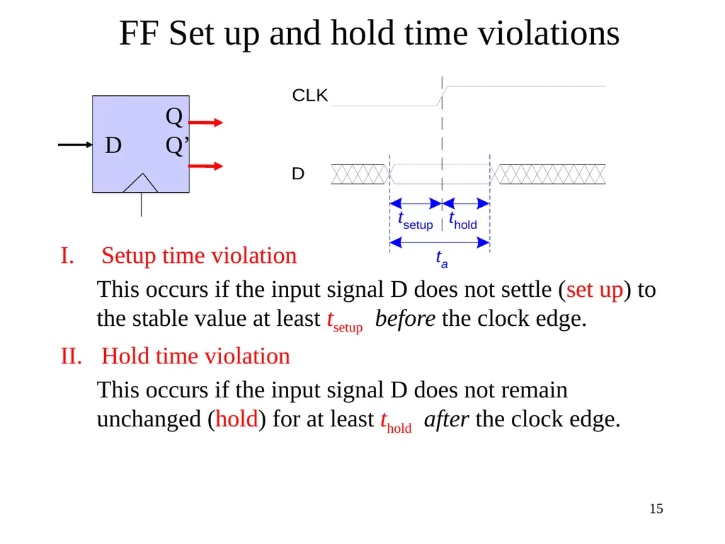
FF Set up and hold time violations 15 Setup time violation
This occurs if the input signal D does not settle (set up) to the stable value at least tsetup before the clock edge.
Hold time violation
This occurs if the input signal D does not remain unchanged (hold) for at least thold after the clock edge.<br>
This occurs if the input signal D does not settle (set up) to the stable value at least tsetup before the clock edge.
Hold time violation
This occurs if the input signal D does not remain unchanged (hold) for at least thold after the clock edge.<br>
16
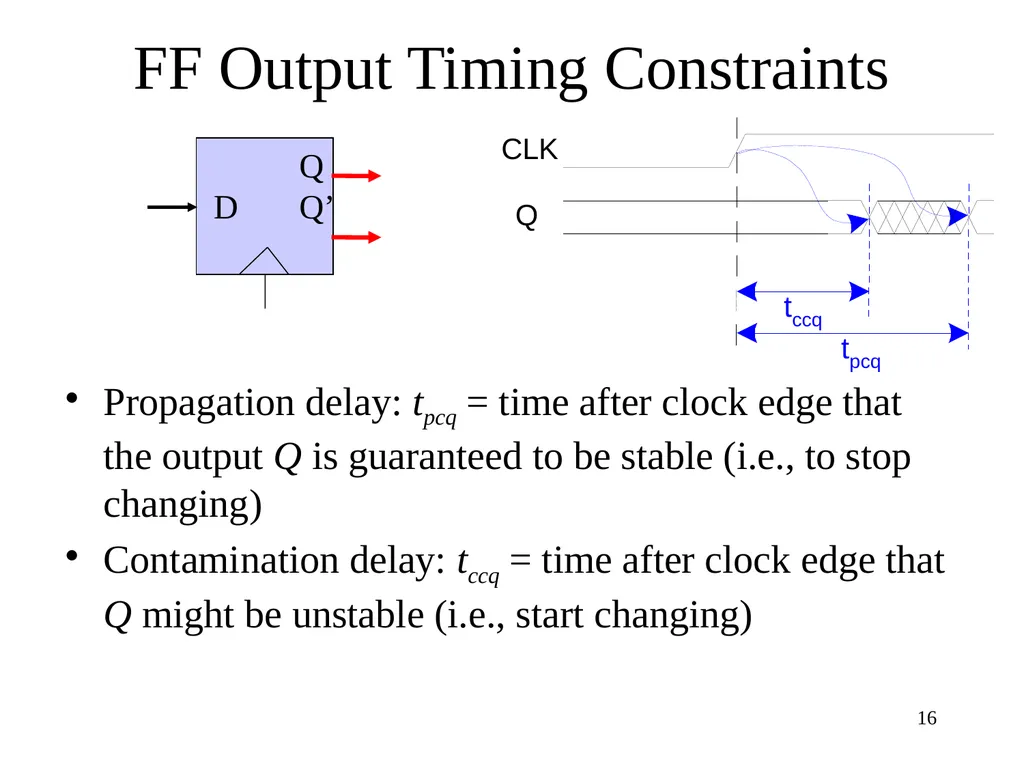
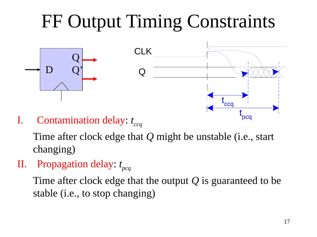
FF Output Timing Constraints Propagation delay: tpcq = time after clock edge that the output Q is guaranteed to be stable (i.e., to stop changing)
Contamination delay: tccq = time after clock edge that Q might be unstable (i.e., start changing) 16<br>
Contamination delay: tccq = time after clock edge that Q might be unstable (i.e., start changing) 16<br>
17
FF Output Timing Constraints Contamination delay: tccq
Time after clock edge that Q might be unstable (i.e., start changing)
Propagation delay: tpcq
Time after clock edge that the output Q is guaranteed to be stable (i.e., to stop changing) 17<br>
Time after clock edge that Q might be unstable (i.e., start changing)
Propagation delay: tpcq
Time after clock edge that the output Q is guaranteed to be stable (i.e., to stop changing) 17<br>
18
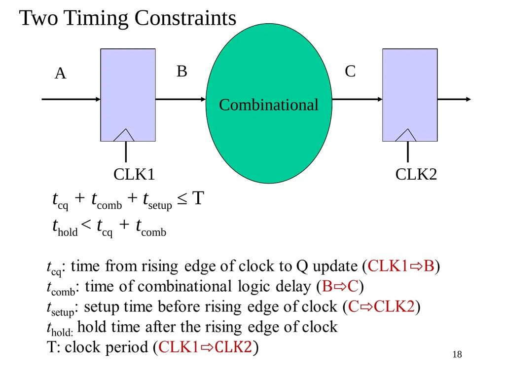
tcq + tcomb + tsetup ≤ T
thold < tcq + tcomb 18 Two Timing Constraints<br>
thold < tcq + tcomb 18 Two Timing Constraints<br>
19
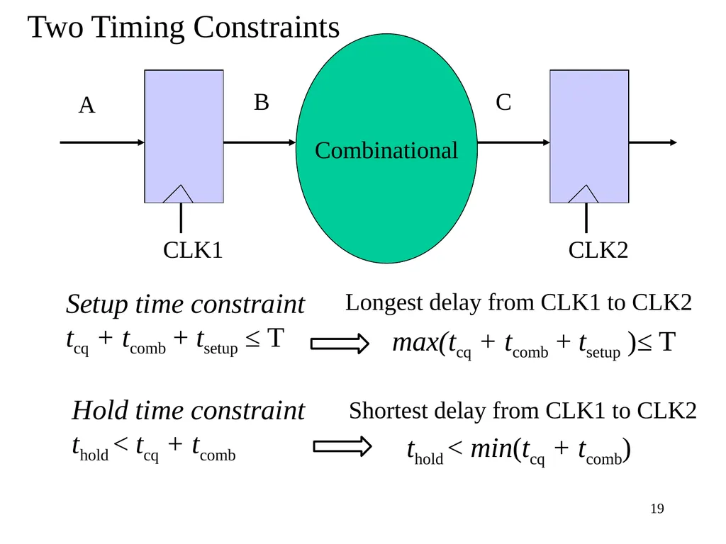
Hold time constraint
thold < tcq + tcomb 19 Setup time constraint
tcq + tcomb + tsetup ≤ T max(tcq + tcomb + tsetup )≤ T thold < min(tcq + tcomb) Longest delay from CLK1 to CLK2 Shortest delay from CLK1 to CLK2 Two Timing Constraints<br>
thold < tcq + tcomb 19 Setup time constraint
tcq + tcomb + tsetup ≤ T max(tcq + tcomb + tsetup )≤ T thold < min(tcq + tcomb) Longest delay from CLK1 to CLK2 Shortest delay from CLK1 to CLK2 Two Timing Constraints<br>
20
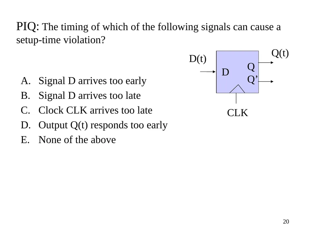
PIQ: The timing of which of the following signals can cause a setup-time violation? Signal D arrives too early
Signal D arrives too late
Clock CLK arrives too late
Output Q(t) responds too early
None of the above 20<br>
Signal D arrives too late
Clock CLK arrives too late
Output Q(t) responds too early
None of the above 20<br>
21
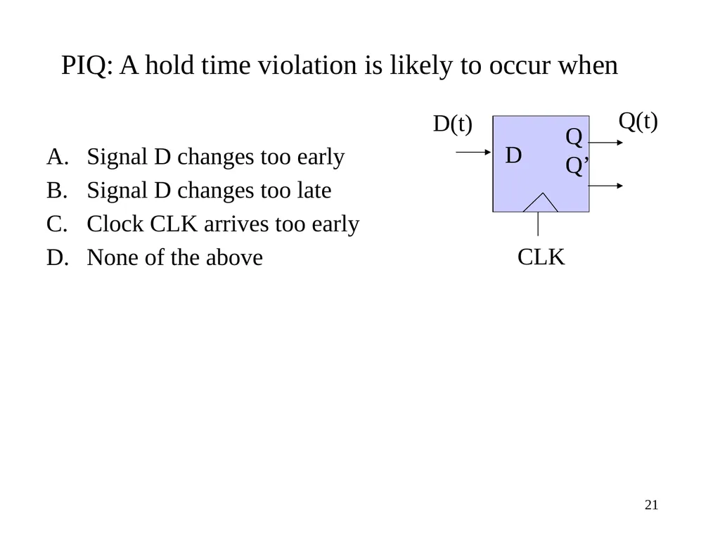
PIQ: A hold time violation is likely to occur when Signal D changes too early
Signal D changes too late
Clock CLK arrives too early
None of the above 21<br>
Signal D changes too late
Clock CLK arrives too early
None of the above 21<br>
22
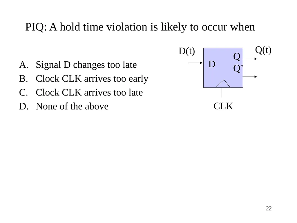
PIQ: A hold time violation is likely to occur when Signal D changes too late
Clock CLK arrives too early
Clock CLK arrives too late
None of the above 22<br>
Clock CLK arrives too early
Clock CLK arrives too late
None of the above 22<br>
23
An alternate view of the sequential circuit<br>
24
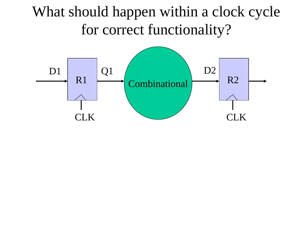
What should happen within a clock cycle for correct functionality?<br>
25
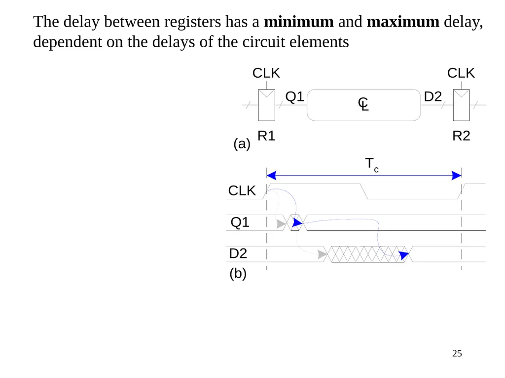
The delay between registers has a minimum and maximum delay, dependent on the delays of the circuit elements 25<br>
26
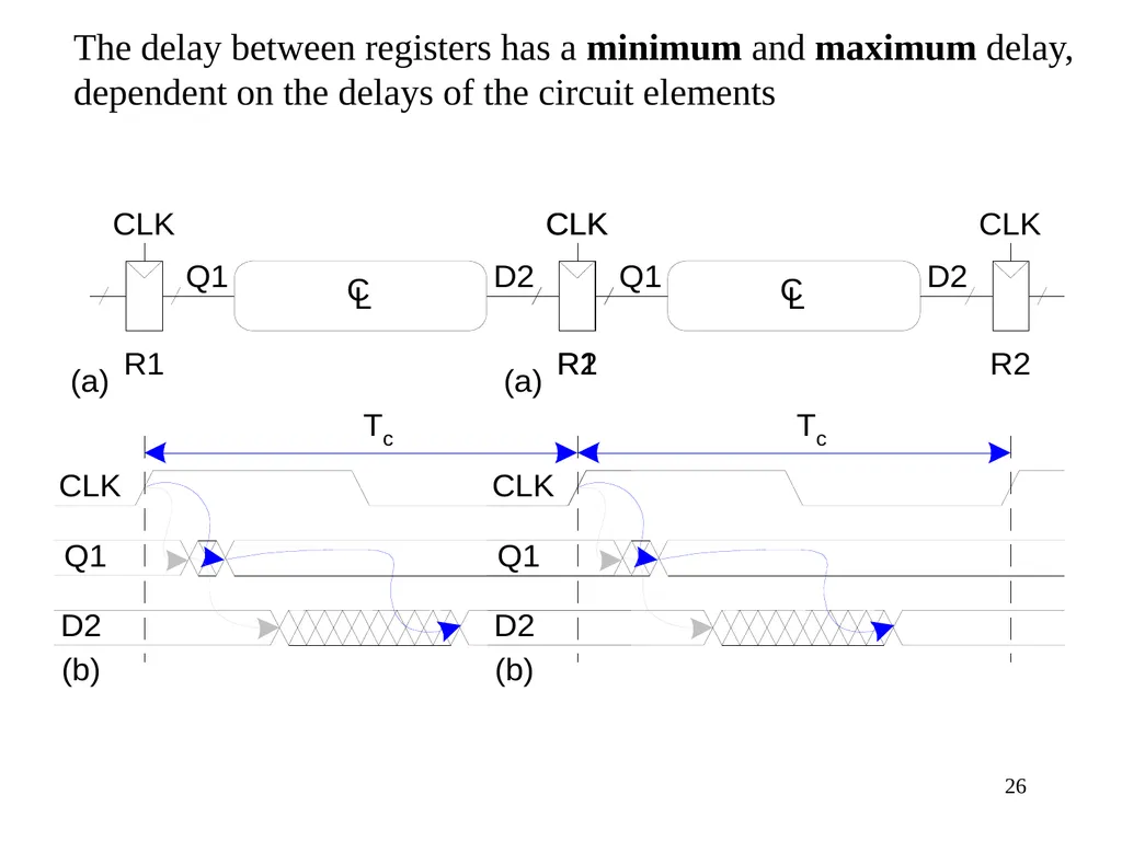
The delay between registers has a minimum and maximum delay, dependent on the delays of the circuit elements 26<br>
27
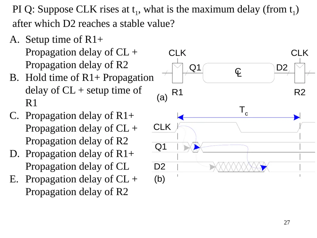
27 PI Q: Suppose CLK rises at t1, what is the maximum delay (from t1) after which D2 reaches a stable value? Setup time of R1+ Propagation delay of CL + Propagation delay of R2
Hold time of R1+ Propagation delay of CL + setup time of R1
Propagation delay of R1+ Propagation delay of CL + Propagation delay of R2
Propagation delay of R1+ Propagation delay of CL
Propagation delay of CL + Propagation delay of R2<br>
Hold time of R1+ Propagation delay of CL + setup time of R1
Propagation delay of R1+ Propagation delay of CL + Propagation delay of R2
Propagation delay of R1+ Propagation delay of CL
Propagation delay of CL + Propagation delay of R2<br>
28
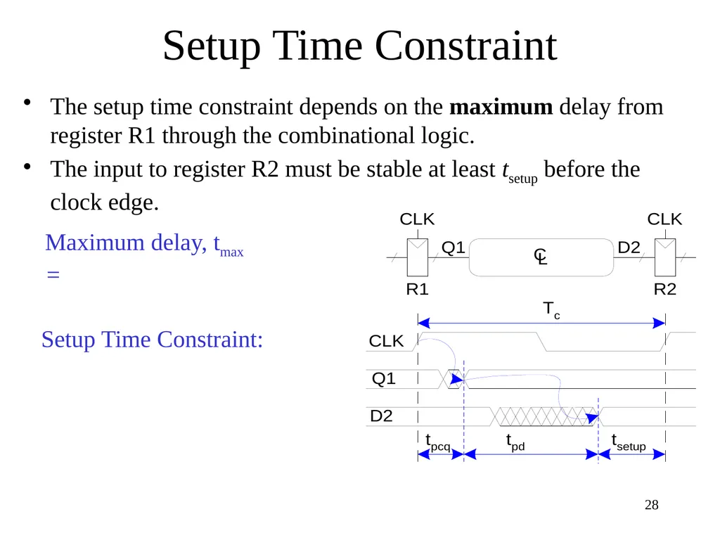
Setup Time Constraint The setup time constraint depends on the maximum delay from register R1 through the combinational logic.
The input to register R2 must be stable at least tsetup before the clock edge. 28 Maximum delay, tmax
= Setup Time Constraint:<br>
The input to register R2 must be stable at least tsetup before the clock edge. 28 Maximum delay, tmax
= Setup Time Constraint:<br>
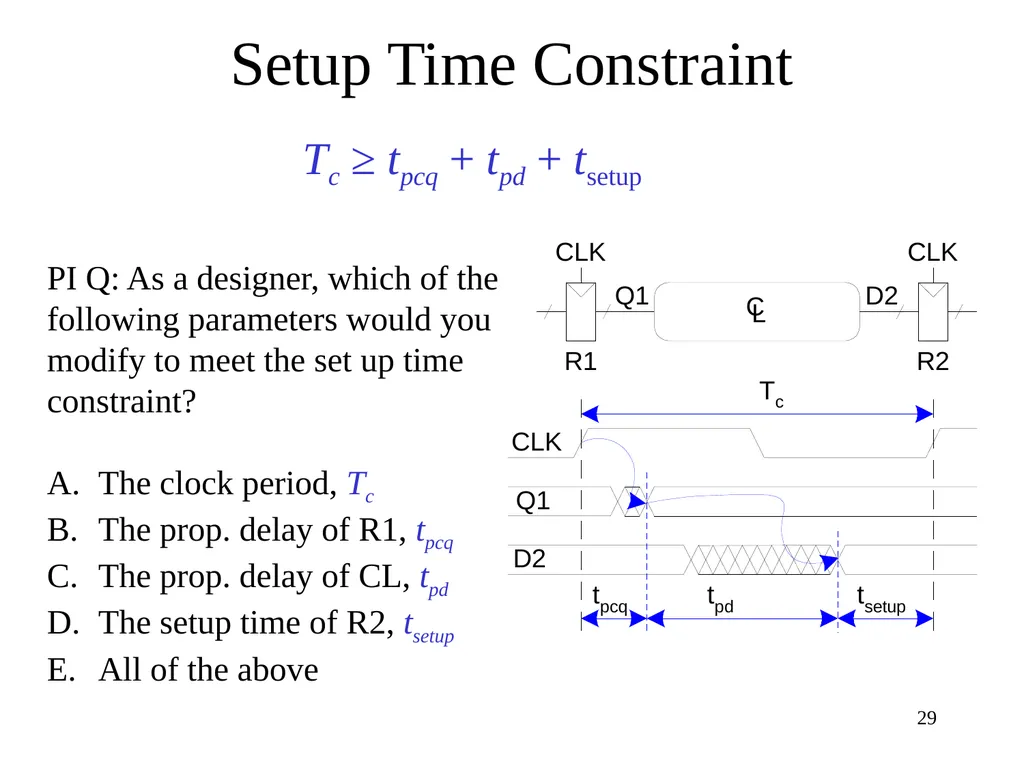
29
Setup Time Constraint Tc ≥ tpcq + tpd + tsetup 29 PI Q: As a designer, which of the following parameters would you modify to meet the set up time constraint?
The clock period, Tc
The prop. delay of R1, tpcq
The prop. delay of CL, tpd
The setup time of R2, tsetup
All of the above<br>
The clock period, Tc
The prop. delay of R1, tpcq
The prop. delay of CL, tpd
The setup time of R2, tsetup
All of the above<br>
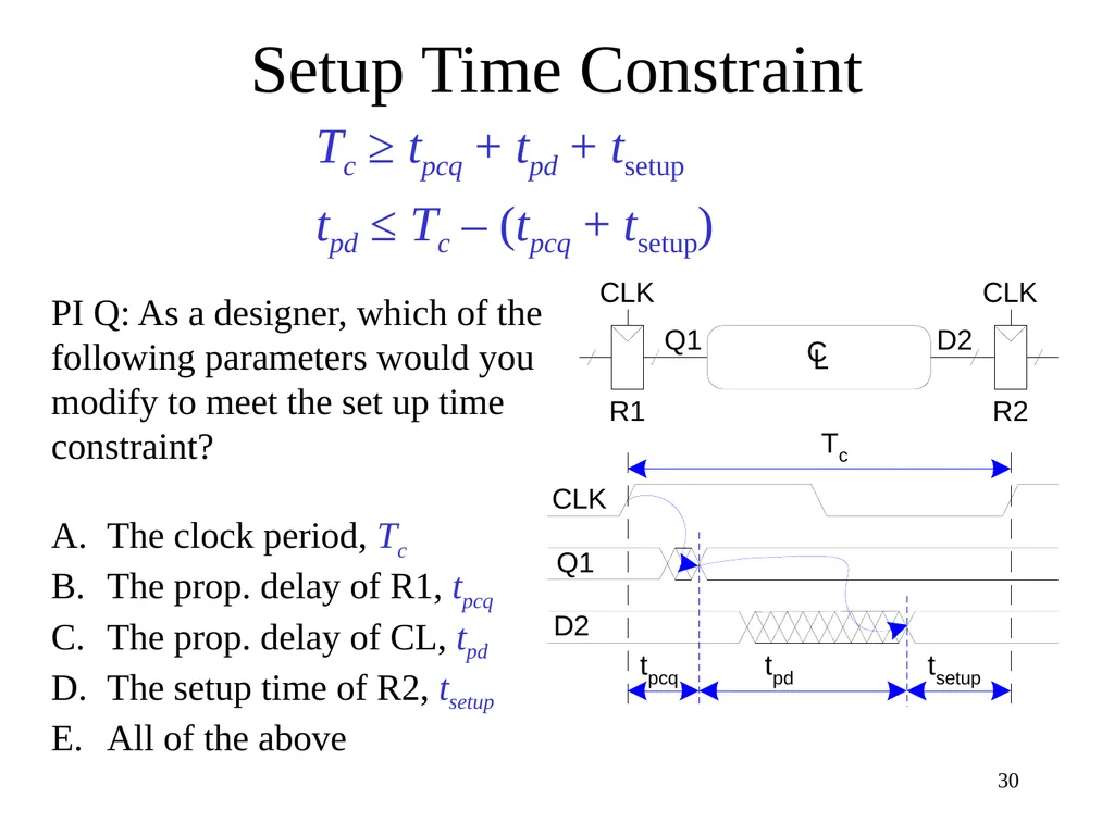
30
Setup Time Constraint 30 PI Q: As a designer, which of the following parameters would you modify to meet the set up time constraint?
The clock period, Tc
The prop. delay of R1, tpcq
The prop. delay of CL, tpd
The setup time of R2, tsetup
All of the above Tc ≥ tpcq + tpd + tsetup
tpd ≤ Tc – (tpcq + tsetup)<br>
The clock period, Tc
The prop. delay of R1, tpcq
The prop. delay of CL, tpd
The setup time of R2, tsetup
All of the above Tc ≥ tpcq + tpd + tsetup
tpd ≤ Tc – (tpcq + tsetup)<br>
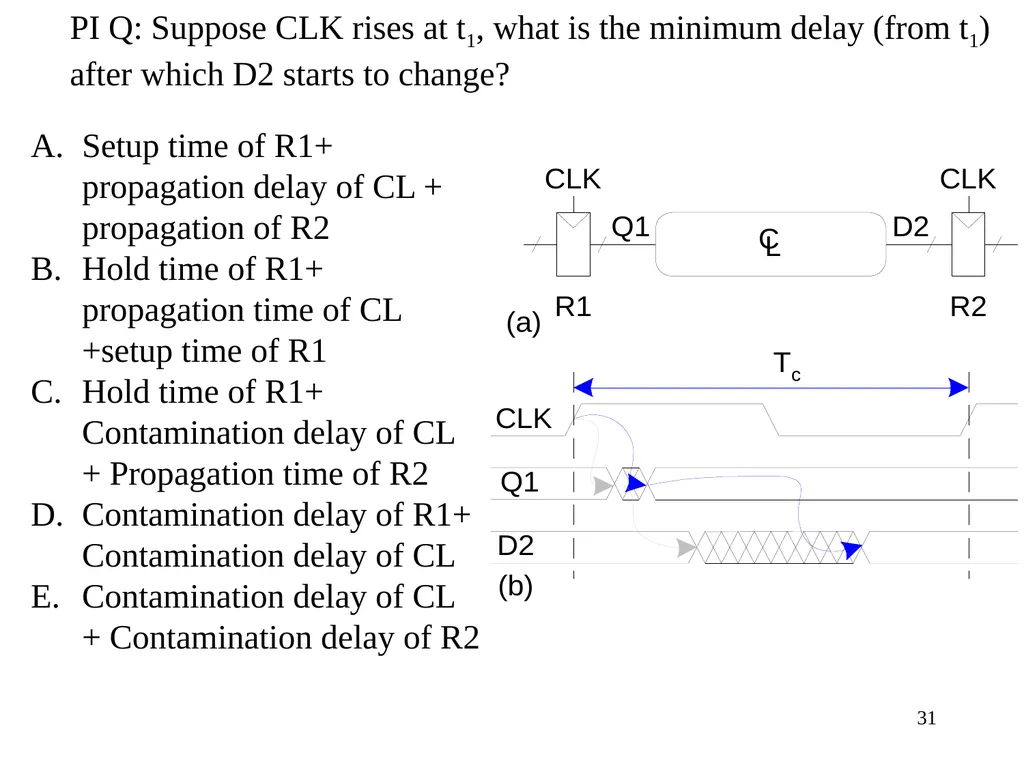
31
31 PI Q: Suppose CLK rises at t1, what is the minimum delay (from t1) after which D2 starts to change? Setup time of R1+ propagation delay of CL + propagation of R2
Hold time of R1+ propagation time of CL +setup time of R1
Hold time of R1+ Contamination delay of CL + Propagation time of R2
Contamination delay of R1+ Contamination delay of CL
Contamination delay of CL + Contamination delay of R2<br>
Hold time of R1+ propagation time of CL +setup time of R1
Hold time of R1+ Contamination delay of CL + Propagation time of R2
Contamination delay of R1+ Contamination delay of CL
Contamination delay of CL + Contamination delay of R2<br>
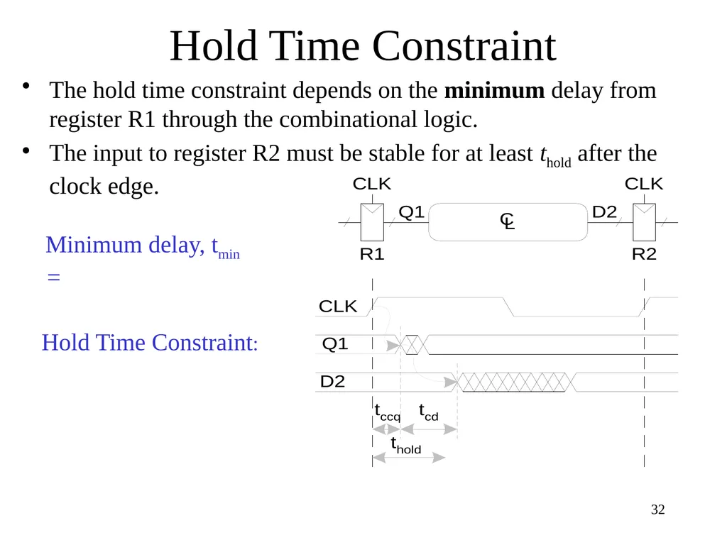
32
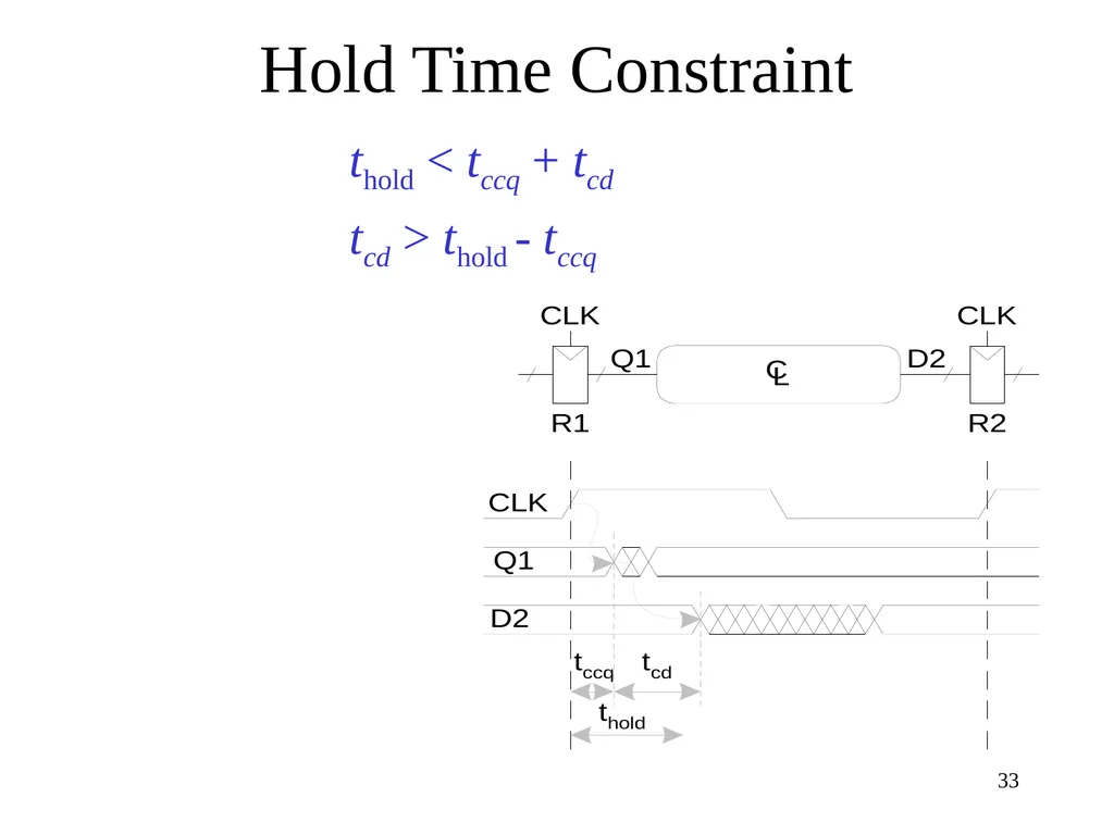
Hold Time Constraint The hold time constraint depends on the minimum delay from register R1 through the combinational logic.
The input to register R2 must be stable for at least thold after the clock edge. 32 Minimum delay, tmin
= Hold Time Constraint:<br>
The input to register R2 must be stable for at least thold after the clock edge. 32 Minimum delay, tmin
= Hold Time Constraint:<br>
33
Hold Time Constraint 33 thold < tccq + tcd
tcd > thold - tccq<br>
tcd > thold - tccq<br>
34
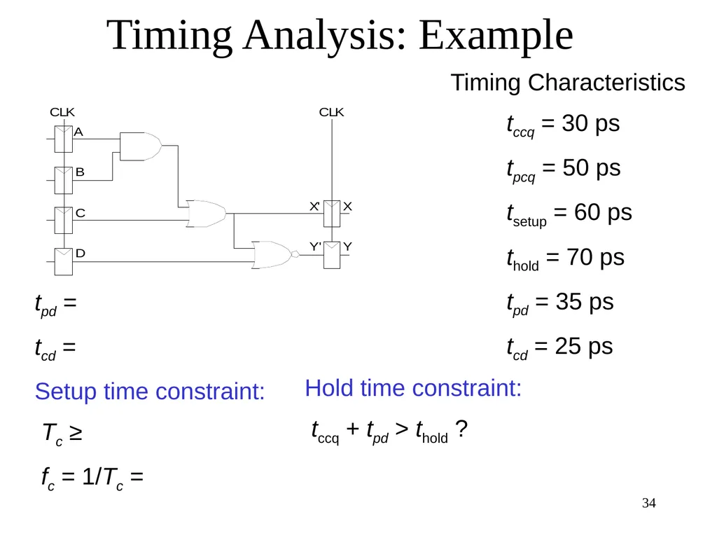
Timing Analysis: Example Timing Characteristics
tccq = 30 ps
tpcq = 50 ps
tsetup = 60 ps
thold = 70 ps
tpd = 35 ps
tcd = 25 ps tpd =
tcd =
Setup time constraint:
Tc ≥
fc = 1/Tc = Hold time constraint:
tccq + tpd > thold ? 34<br>
tccq = 30 ps
tpcq = 50 ps
tsetup = 60 ps
thold = 70 ps
tpd = 35 ps
tcd = 25 ps tpd =
tcd =
Setup time constraint:
Tc ≥
fc = 1/Tc = Hold time constraint:
tccq + tpd > thold ? 34<br>
35
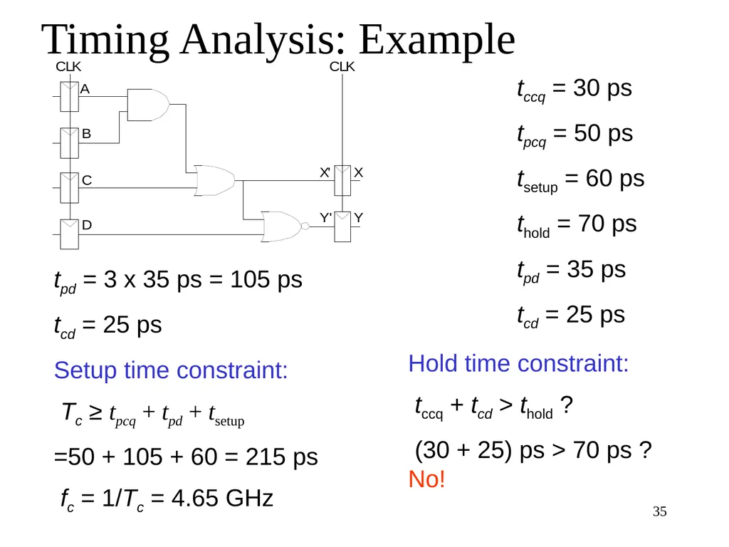
Timing Analysis: Example tccq = 30 ps
tpcq = 50 ps
tsetup = 60 ps
thold = 70 ps
tpd = 35 ps
tcd = 25 ps 35 tpd = 3 x 35 ps = 105 ps
tcd = 25 ps
Setup time constraint:
Tc ≥ tpcq + tpd + tsetup
=50 + 105 + 60 = 215 ps
fc = 1/Tc = 4.65 GHz Hold time constraint:
tccq + tcd > thold ?
(30 + 25) ps > 70 ps ? No!<br>
tpcq = 50 ps
tsetup = 60 ps
thold = 70 ps
tpd = 35 ps
tcd = 25 ps 35 tpd = 3 x 35 ps = 105 ps
tcd = 25 ps
Setup time constraint:
Tc ≥ tpcq + tpd + tsetup
=50 + 105 + 60 = 215 ps
fc = 1/Tc = 4.65 GHz Hold time constraint:
tccq + tcd > thold ?
(30 + 25) ps > 70 ps ? No!<br>
36
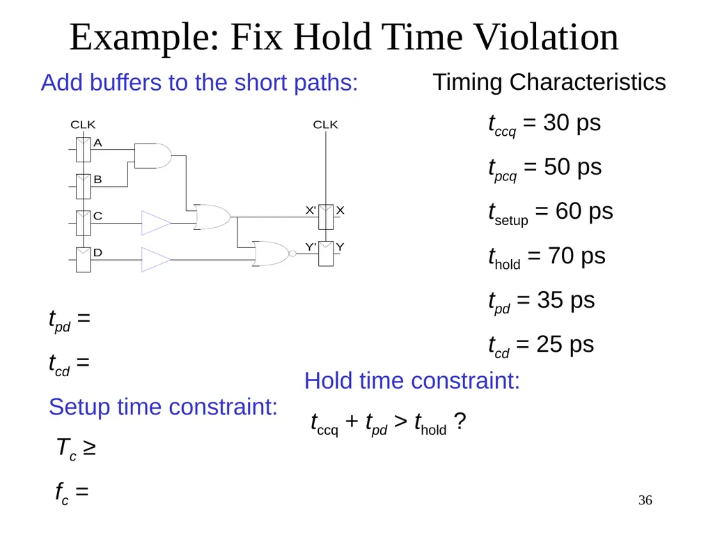
Example: Fix Hold Time Violation Timing Characteristics
tccq = 30 ps
tpcq = 50 ps
tsetup = 60 ps
thold = 70 ps
tpd = 35 ps
tcd = 25 ps tpd =
tcd =
Setup time constraint:
Tc ≥
fc = Hold time constraint:
tccq + tpd > thold ? Add buffers to the short paths: 36<br>
tccq = 30 ps
tpcq = 50 ps
tsetup = 60 ps
thold = 70 ps
tpd = 35 ps
tcd = 25 ps tpd =
tcd =
Setup time constraint:
Tc ≥
fc = Hold time constraint:
tccq + tpd > thold ? Add buffers to the short paths: 36<br>
37
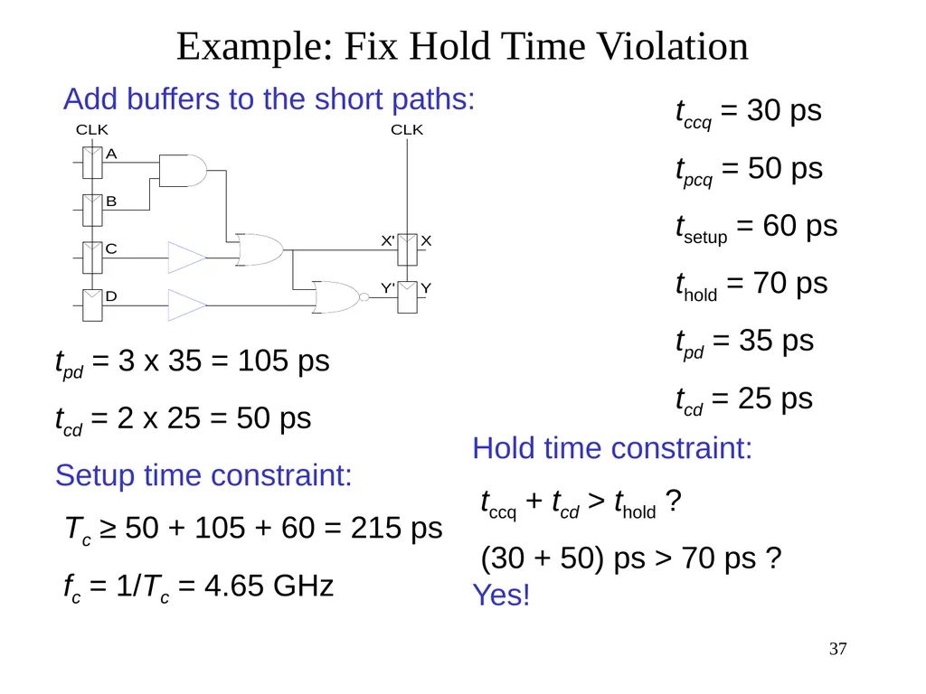
Example: Fix Hold Time Violation tccq = 30 ps
tpcq = 50 ps
tsetup = 60 ps
thold = 70 ps
tpd = 35 ps
tcd = 25 ps tpd = 3 x 35 = 105 ps
tcd = 2 x 25 = 50 ps
Setup time constraint:
Tc ≥ 50 + 105 + 60 = 215 ps
fc = 1/Tc = 4.65 GHz Hold time constraint:
tccq + tcd > thold ?
(30 + 50) ps > 70 ps ? Yes! Add buffers to the short paths: 37<br>
tpcq = 50 ps
tsetup = 60 ps
thold = 70 ps
tpd = 35 ps
tcd = 25 ps tpd = 3 x 35 = 105 ps
tcd = 2 x 25 = 50 ps
Setup time constraint:
Tc ≥ 50 + 105 + 60 = 215 ps
fc = 1/Tc = 4.65 GHz Hold time constraint:
tccq + tcd > thold ?
(30 + 50) ps > 70 ps ? Yes! Add buffers to the short paths: 37<br>
38
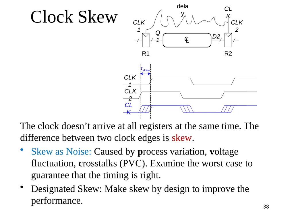
Clock Skew The clock doesn’t arrive at all registers at the same time. The difference between two clock edges is skew.
Skew as Noise: Caused by process variation, voltage fluctuation, crosstalks (PVC). Examine the worst case to guarantee that the timing is right.
Designated Skew: Make skew by design to improve the performance. 38<br>
Skew as Noise: Caused by process variation, voltage fluctuation, crosstalks (PVC). Examine the worst case to guarantee that the timing is right.
Designated Skew: Make skew by design to improve the performance. 38<br>
39
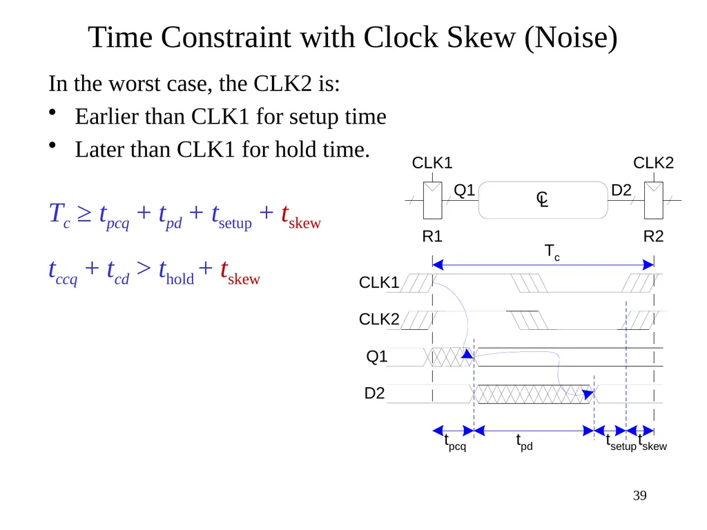
Time Constraint with Clock Skew (Noise) In the worst case, the CLK2 is:
Earlier than CLK1 for setup time
Later than CLK1 for hold time. Tc ≥ tpcq + tpd + tsetup + tskew 39 tccq + tcd > thold + tskew<br>
Earlier than CLK1 for setup time
Later than CLK1 for hold time. Tc ≥ tpcq + tpd + tsetup + tskew 39 tccq + tcd > thold + tskew<br>
40
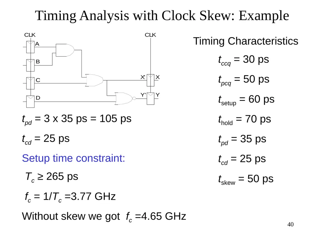
Timing Analysis with Clock Skew: Example Timing Characteristics
tccq = 30 ps
tpcq = 50 ps
tsetup = 60 ps
thold = 70 ps
tpd = 35 ps
tcd = 25 ps
tskew = 50 ps tpd = 3 x 35 ps = 105 ps
tcd = 25 ps
Setup time constraint:
Tc ≥ 265 ps
fc = 1/Tc =3.77 GHz
Without skew we got fc =4.65 GHz 40<br>
tccq = 30 ps
tpcq = 50 ps
tsetup = 60 ps
thold = 70 ps
tpd = 35 ps
tcd = 25 ps
tskew = 50 ps tpd = 3 x 35 ps = 105 ps
tcd = 25 ps
Setup time constraint:
Tc ≥ 265 ps
fc = 1/Tc =3.77 GHz
Without skew we got fc =4.65 GHz 40<br>
41
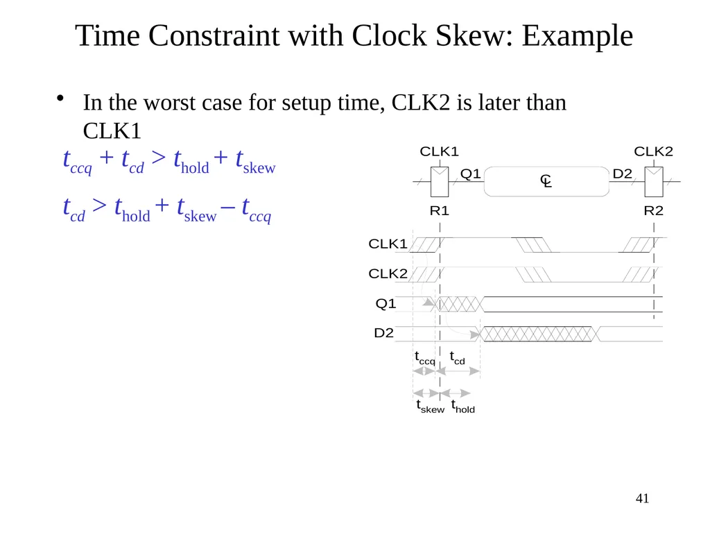
Time Constraint with Clock Skew: Example In the worst case for setup time, CLK2 is later than CLK1 tccq + tcd > thold + tskew
tcd > thold + tskew – tccq 41<br>
tcd > thold + tskew – tccq 41<br>
42
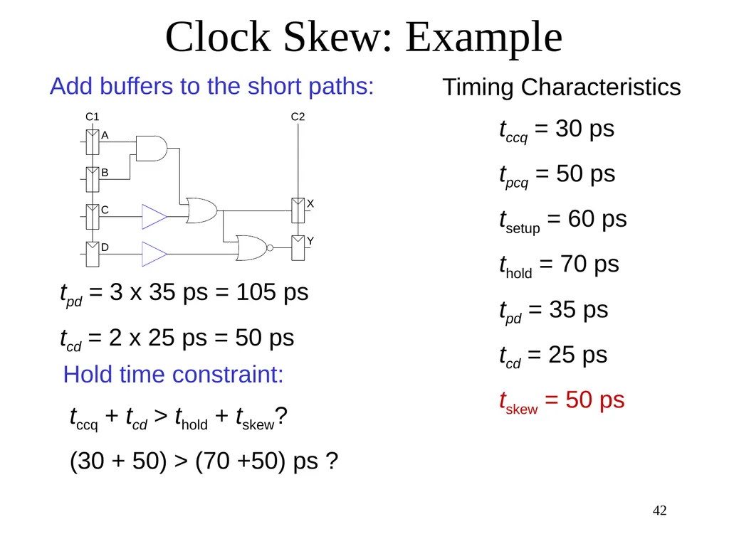
Clock Skew: Example Timing Characteristics
tccq = 30 ps
tpcq = 50 ps
tsetup = 60 ps
thold = 70 ps
tpd = 35 ps
tcd = 25 ps
tskew = 50 ps tpd = 3 x 35 ps = 105 ps
tcd = 2 x 25 ps = 50 ps Hold time constraint:
tccq + tcd > thold + tskew?
(30 + 50) > (70 +50) ps ? Add buffers to the short paths: 42<br>
tccq = 30 ps
tpcq = 50 ps
tsetup = 60 ps
thold = 70 ps
tpd = 35 ps
tcd = 25 ps
tskew = 50 ps tpd = 3 x 35 ps = 105 ps
tcd = 2 x 25 ps = 50 ps Hold time constraint:
tccq + tcd > thold + tskew?
(30 + 50) > (70 +50) ps ? Add buffers to the short paths: 42<br>
43
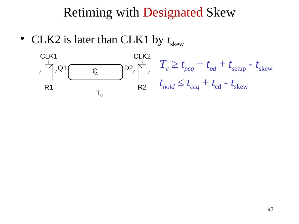
Retiming with Designated Skew CLK2 is later than CLK1 by tskew Tc ≥ tpcq + tpd + tsetup - tskew
thold ≤ tccq + tcd - tskew 43<br>
thold ≤ tccq + tcd - tskew 43<br>
44
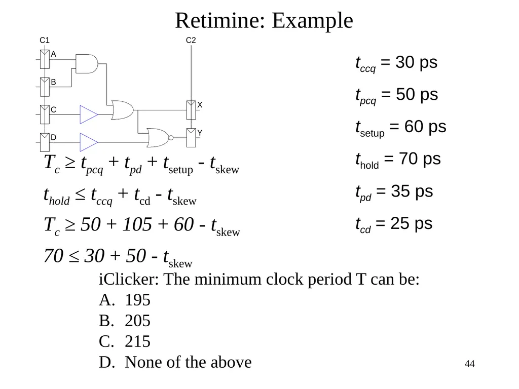
Retimine: Example tccq = 30 ps
tpcq = 50 ps
tsetup = 60 ps
thold = 70 ps
tpd = 35 ps
tcd = 25 ps 44 Tc ≥ tpcq + tpd + tsetup - tskew
thold ≤ tccq + tcd - tskew Tc ≥ 50 + 105 + 60 - tskew
70 ≤ 30 + 50 - tskew iClicker: The minimum clock period T can be:
195
205
215
None of the above<br>
tpcq = 50 ps
tsetup = 60 ps
thold = 70 ps
tpd = 35 ps
tcd = 25 ps 44 Tc ≥ tpcq + tpd + tsetup - tskew
thold ≤ tccq + tcd - tskew Tc ≥ 50 + 105 + 60 - tskew
70 ≤ 30 + 50 - tskew iClicker: The minimum clock period T can be:
195
205
215
None of the above<br>
45
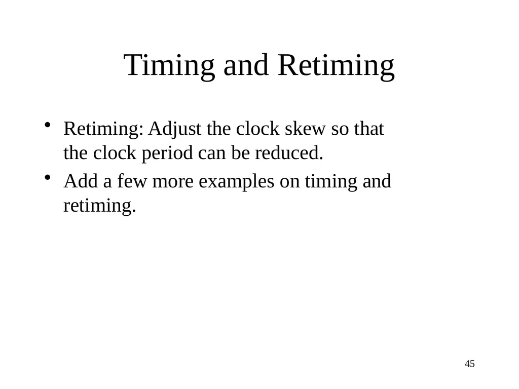
Timing and Retiming Retiming: Adjust the clock skew so that the clock period can be reduced.
Add a few more examples on timing and retiming. 45<br>
Add a few more examples on timing and retiming. 45<br>
46
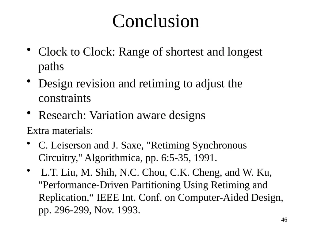
Conclusion Clock to Clock: Range of shortest and longest paths
Design revision and retiming to adjust the constraints
Research: Variation aware designs
Extra materials:
C. Leiserson and J. Saxe, "Retiming Synchronous Circuitry," Algorithmica, pp. 6:5-35, 1991.
L.T. Liu, M. Shih, N.C. Chou, C.K. Cheng, and W. Ku, "Performance-Driven Partitioning Using Retiming and Replication,“ IEEE Int. Conf. on Computer-Aided Design, pp. 296-299, Nov. 1993. 46<br>
Design revision and retiming to adjust the constraints
Research: Variation aware designs
Extra materials:
C. Leiserson and J. Saxe, "Retiming Synchronous Circuitry," Algorithmica, pp. 6:5-35, 1991.
L.T. Liu, M. Shih, N.C. Chou, C.K. Cheng, and W. Ku, "Performance-Driven Partitioning Using Retiming and Replication,“ IEEE Int. Conf. on Computer-Aided Design, pp. 296-299, Nov. 1993. 46<br>